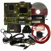
R0K572030S000BE Renesas Electronics America, R0K572030S000BE Datasheet - Page 263

R0K572030S000BE
Manufacturer Part Number
R0K572030S000BE
Description
KIT DEV FOR SH7203
Manufacturer
Renesas Electronics America
Series
Renesas Starter Kits (RSK)r
Type
MCUr
Specifications of R0K572030S000BE
Contents
CPU Board, LCD Module, E10A-Lite Emulator, Cable, QuickStart Guide and CD-ROM
Silicon Manufacturer
Renesas
Kit Contents
Board
Silicon Family Name
SH7203
Silicon Core Number
R5S72030W200FP
Tool / Board Applications
General Purpose MCU, MPU, DSP, DSC
Mcu Supported Families
SH7203
Lead Free Status / RoHS Status
Contains lead / RoHS non-compliant
For Use With/related Products
SH7203
Lead Free Status / Rohs Status
Compliant
- Current page: 263 of 1686
- Download datasheet (10Mb)
8.3.4
(1)
In a write access in write-back mode, the data is written to the cache and no external memory
write cycle is issued. The U bit of the entry written is set to 1 and LRU is updated so that the hit
way becomes the latest.
In write-through mode, the data is written to the cache and an external memory write cycle is
issued. The U bit of the written entry is not updated and LRU is updated so that the replaced way
becomes the latest.
(2)
In write-back mode, an external bus cycle starts when a write miss occurs, and the entry is
updated. The way to be replaced follows table 8.4. When the U bit of the entry to be replaced is 1,
the cache update cycle starts after the entry is transferred to the write-back buffer. Data is written
to the cache, the U bit is set to 1, and the V bit is set to 1. LRU is updated so that the replaced way
becomes the latest. After the cache completes its update cycle, the write-back buffer writes the
entry back to the memory. The write-back unit is 16 bytes. Cache updates and write-backs to
memory are performed in wrap-around fashion. For example, if the value of the lower four bits of
an address that triggers a write miss is H'4, the value of the lower four address bits changes from
H'4 to H'8, H'C, and H'0, in that order, when cache updates or write-backs are performed.
In write-through mode, no write to cache occurs in a write miss; the write is only to the external
memory.
8.3.5
When the U bit of the entry to be replaced in the write-back mode is 1, it must be written back to
the external memory. To increase performance, the entry to be replaced is first transferred to the
write-back buffer and fetching of new entries to the cache takes priority over writing back to the
external memory. After the cache completes to fetch the new entry, the write-back buffer writes
the entry back to external memory. During the write-back cycles, the cache can be accessed. The
write-back buffer can hold one line of cache data (16 bytes) and its physical address. Figure 8.3
shows the configuration of the write-back buffer.
Write Hit
Write Miss
Write Operation (Only for Operand Cache)
Write-Back Buffer (Only for Operand Cache)
A (31 to 4):
Longword 0 to 3:
A (31 to 4)
Figure 8.3 Write-Back Buffer Configuration
Longword 0
Physical address written to external memory (upper three bits are 0)
One line of cache data to be written to external memory
Longword 1
Longword 2
Rev. 3.00 Sep. 28, 2009 Page 231 of 1650
Longword 3
REJ09B0313-0300
Section 8 Cache
Related parts for R0K572030S000BE
Image
Part Number
Description
Manufacturer
Datasheet
Request
R

Part Number:
Description:
KIT STARTER FOR M16C/29
Manufacturer:
Renesas Electronics America
Datasheet:

Part Number:
Description:
KIT STARTER FOR R8C/2D
Manufacturer:
Renesas Electronics America
Datasheet:

Part Number:
Description:
R0K33062P STARTER KIT
Manufacturer:
Renesas Electronics America
Datasheet:

Part Number:
Description:
KIT STARTER FOR R8C/23 E8A
Manufacturer:
Renesas Electronics America
Datasheet:

Part Number:
Description:
KIT STARTER FOR R8C/25
Manufacturer:
Renesas Electronics America
Datasheet:

Part Number:
Description:
KIT STARTER H8S2456 SHARPE DSPLY
Manufacturer:
Renesas Electronics America
Datasheet:

Part Number:
Description:
KIT STARTER FOR R8C38C
Manufacturer:
Renesas Electronics America
Datasheet:

Part Number:
Description:
KIT STARTER FOR R8C35C
Manufacturer:
Renesas Electronics America
Datasheet:

Part Number:
Description:
KIT STARTER FOR R8CL3AC+LCD APPS
Manufacturer:
Renesas Electronics America
Datasheet:

Part Number:
Description:
KIT STARTER FOR RX610
Manufacturer:
Renesas Electronics America
Datasheet:

Part Number:
Description:
KIT STARTER FOR R32C/118
Manufacturer:
Renesas Electronics America
Datasheet:

Part Number:
Description:
KIT DEV RSK-R8C/26-29
Manufacturer:
Renesas Electronics America
Datasheet:

Part Number:
Description:
KIT STARTER FOR SH7124
Manufacturer:
Renesas Electronics America
Datasheet:

Part Number:
Description:
KIT STARTER FOR H8SX/1622
Manufacturer:
Renesas Electronics America
Datasheet:

Part Number:
Description:
KIT STARTER FOR R8C/18191A1B
Manufacturer:
Renesas Electronics America
Datasheet:


