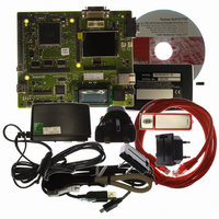
R0K572030S000BE Renesas Electronics America, R0K572030S000BE Datasheet - Page 1460

R0K572030S000BE
Manufacturer Part Number
R0K572030S000BE
Description
KIT DEV FOR SH7203
Manufacturer
Renesas Electronics America
Series
Renesas Starter Kits (RSK)r
Type
MCUr
Specifications of R0K572030S000BE
Contents
CPU Board, LCD Module, E10A-Lite Emulator, Cable, QuickStart Guide and CD-ROM
Silicon Manufacturer
Renesas
Kit Contents
Board
Silicon Family Name
SH7203
Silicon Core Number
R5S72030W200FP
Tool / Board Applications
General Purpose MCU, MPU, DSP, DSC
Mcu Supported Families
SH7203
Lead Free Status / RoHS Status
Contains lead / RoHS non-compliant
For Use With/related Products
SH7203
Lead Free Status / Rohs Status
Compliant
- Current page: 1460 of 1686
- Download datasheet (10Mb)
Section 28 Power-Down Modes
28.3.4
(1)
The LSI switches from a program execution state to deep standby mode by executing the SLEEP
instruction when the STBY bit and DEEP bit in STBCR are set to 1. In deep standby mode, not
only the CPU, clocks, and on-chip peripheral modules but also power supply is turned off
excluding the on-chip RAM (for data retention) retaining area specified by the RRAMKP3 to
RRAMKP0 bits in DSCTR and RTC. This can significantly reduce power consumption.
Therefore, data in the registers of the CPU, cache, and on-chip peripheral modules are not
retained. Pin state values immediately before the transition to deep standby mode are retained.
The CPU takes one cycle to finish writing to DSCTR, and then executes processing for the next
instruction. However, it actually takes one or more cycles to write. Therefore, execute a SLEEP
instruction after reading DSCTR to reflect the values written to DSCTR by the CPU in the SLEEP
instruction without fail.
The procedure for switching to deep standby mode is as follows. Figure 28.2 also shows its
flowchart.
1. To ensure that data is actually retained in deep standby mode by the on-chip RAM (for data
2. Set the RRAMKP3 to RRAMKP0 bits in DSCTR for the corresponding on-chip RAM (for
3. To cancel deep standby mode by an interrupt, set to 1 the bit in DSSSR corresponding to the
4. Execute read and write of an arbitrary but the same address for each page in the retaining on-
5. Set the STBY and DEEP bits in the STBCR register to 1.
6. Read out the DSFR register after clearing the flag in the DSFR register. Then execute the
Rev. 3.00 Sep. 28, 2009 Page 1428 of 1650
REJ09B0313-0300
retention), set H'09 to DSRTR.
data retention) area that must be retained. Transfer the programs to be retained to the specified
areas of the on-chip RAM (for data retention).
pin to be used for cancellation. In this case, also set the input signal detection mode (using
interrupt control registers 0 and 1 (ICR0 and ICR1) of the interrupt controller (INTC)) for the
pin used for cancellation. In the case of deep standby mode, only rising- or falling-edge
detection is valid. (Low-level detection or both-edge detection of the IRQ signal cannot be
used to cancel deep standby mode.)
chip RAM (for data retention) area. When this is not executed, data last written may not be
written to the on-chip RAM (for data retention). If there is a write to the on-chip RAM (for
data retention) after this time, execute this processing after the last write to the on-chip RAM
(for data retention).
SLEEP instruction.
Transition to Deep Standby Mode
Deep Standby Mode
Related parts for R0K572030S000BE
Image
Part Number
Description
Manufacturer
Datasheet
Request
R

Part Number:
Description:
KIT STARTER FOR M16C/29
Manufacturer:
Renesas Electronics America
Datasheet:

Part Number:
Description:
KIT STARTER FOR R8C/2D
Manufacturer:
Renesas Electronics America
Datasheet:

Part Number:
Description:
R0K33062P STARTER KIT
Manufacturer:
Renesas Electronics America
Datasheet:

Part Number:
Description:
KIT STARTER FOR R8C/23 E8A
Manufacturer:
Renesas Electronics America
Datasheet:

Part Number:
Description:
KIT STARTER FOR R8C/25
Manufacturer:
Renesas Electronics America
Datasheet:

Part Number:
Description:
KIT STARTER H8S2456 SHARPE DSPLY
Manufacturer:
Renesas Electronics America
Datasheet:

Part Number:
Description:
KIT STARTER FOR R8C38C
Manufacturer:
Renesas Electronics America
Datasheet:

Part Number:
Description:
KIT STARTER FOR R8C35C
Manufacturer:
Renesas Electronics America
Datasheet:

Part Number:
Description:
KIT STARTER FOR R8CL3AC+LCD APPS
Manufacturer:
Renesas Electronics America
Datasheet:

Part Number:
Description:
KIT STARTER FOR RX610
Manufacturer:
Renesas Electronics America
Datasheet:

Part Number:
Description:
KIT STARTER FOR R32C/118
Manufacturer:
Renesas Electronics America
Datasheet:

Part Number:
Description:
KIT DEV RSK-R8C/26-29
Manufacturer:
Renesas Electronics America
Datasheet:

Part Number:
Description:
KIT STARTER FOR SH7124
Manufacturer:
Renesas Electronics America
Datasheet:

Part Number:
Description:
KIT STARTER FOR H8SX/1622
Manufacturer:
Renesas Electronics America
Datasheet:

Part Number:
Description:
KIT STARTER FOR R8C/18191A1B
Manufacturer:
Renesas Electronics America
Datasheet:


