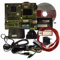
R0K572030S000BE Renesas Electronics America, R0K572030S000BE Datasheet - Page 36

R0K572030S000BE
Manufacturer Part Number
R0K572030S000BE
Description
KIT DEV FOR SH7203
Manufacturer
Renesas Electronics America
Series
Renesas Starter Kits (RSK)r
Type
MCUr
Specifications of R0K572030S000BE
Contents
CPU Board, LCD Module, E10A-Lite Emulator, Cable, QuickStart Guide and CD-ROM
Silicon Manufacturer
Renesas
Kit Contents
Board
Silicon Family Name
SH7203
Silicon Core Number
R5S72030W200FP
Tool / Board Applications
General Purpose MCU, MPU, DSP, DSC
Mcu Supported Families
SH7203
Lead Free Status / RoHS Status
Contains lead / RoHS non-compliant
For Use With/related Products
SH7203
Lead Free Status / Rohs Status
Compliant
- Current page: 36 of 1686
- Download datasheet (10Mb)
Section 1 Overview
Rev. 3.00 Sep. 28, 2009 Page 4 of 1650
REJ09B0313-0300
Items
Bus state controller
(BSC)
Direct memory access
controller (DMAC)
Clock pulse generator
(CPG)
Watchdog timer
(WDT)
Specification
•
•
•
•
•
•
•
•
•
•
•
•
•
•
Address space divided into eight areas (0 to 7), each a maximum of 64
Mbytes
The following features settable for each area independently
⎯ Bus size (8, 16, or 32 bits): Available sizes depend on the area.
⎯ Number of access wait cycles (different wait cycles can be
⎯ Idle wait cycle insertion (between same area access cycles or
⎯ Specifying the memory to be connected to each area enables
⎯ PCMCIA interface
⎯ Outputs a chip select signal (CS0 to CS7) according to the target
SDRAM refresh
Auto refresh or self refresh mode selectable
SDRAM burst access
Eight channels; external request available for four of them
Can be activated by on-chip peripheral modules
Burst mode and cycle steal mode
Intermittent mode available (16 and 64 cycles supported)
Transfer information can be automatically reloaded
Clock mode: Input clock can be selected from external input (EXTAL,
CKIO, or USB_X1) or crystal resonator
Input clock can be multiplied by 16 (max.) by the internal PLL circuit
Three types of clocks generated:
⎯ CPU clock: Maximum 200 MHz
⎯ Bus clock: Maximum 66 MHz
⎯ Peripheral clock: Maximum 33 MHz
On-chip one-channel watchdog timer
A counter overflow can reset the LSI
specified for read and write access cycles in some areas)
different area access cycles)
direct connection to SRAM, SRAM with byte selection, SDRAM,
and burst ROM (clocked synchronous or asynchronous). The
address/data multiplexed I/O (MPX) interface and burst MPX-I/O
interface are also available.
area (CS assert or negate timing can be selected by software)
Related parts for R0K572030S000BE
Image
Part Number
Description
Manufacturer
Datasheet
Request
R

Part Number:
Description:
KIT STARTER FOR M16C/29
Manufacturer:
Renesas Electronics America
Datasheet:

Part Number:
Description:
KIT STARTER FOR R8C/2D
Manufacturer:
Renesas Electronics America
Datasheet:

Part Number:
Description:
R0K33062P STARTER KIT
Manufacturer:
Renesas Electronics America
Datasheet:

Part Number:
Description:
KIT STARTER FOR R8C/23 E8A
Manufacturer:
Renesas Electronics America
Datasheet:

Part Number:
Description:
KIT STARTER FOR R8C/25
Manufacturer:
Renesas Electronics America
Datasheet:

Part Number:
Description:
KIT STARTER H8S2456 SHARPE DSPLY
Manufacturer:
Renesas Electronics America
Datasheet:

Part Number:
Description:
KIT STARTER FOR R8C38C
Manufacturer:
Renesas Electronics America
Datasheet:

Part Number:
Description:
KIT STARTER FOR R8C35C
Manufacturer:
Renesas Electronics America
Datasheet:

Part Number:
Description:
KIT STARTER FOR R8CL3AC+LCD APPS
Manufacturer:
Renesas Electronics America
Datasheet:

Part Number:
Description:
KIT STARTER FOR RX610
Manufacturer:
Renesas Electronics America
Datasheet:

Part Number:
Description:
KIT STARTER FOR R32C/118
Manufacturer:
Renesas Electronics America
Datasheet:

Part Number:
Description:
KIT DEV RSK-R8C/26-29
Manufacturer:
Renesas Electronics America
Datasheet:

Part Number:
Description:
KIT STARTER FOR SH7124
Manufacturer:
Renesas Electronics America
Datasheet:

Part Number:
Description:
KIT STARTER FOR H8SX/1622
Manufacturer:
Renesas Electronics America
Datasheet:

Part Number:
Description:
KIT STARTER FOR R8C/18191A1B
Manufacturer:
Renesas Electronics America
Datasheet:


