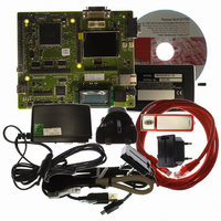
R0K572030S000BE Renesas Electronics America, R0K572030S000BE Datasheet - Page 1426

R0K572030S000BE
Manufacturer Part Number
R0K572030S000BE
Description
KIT DEV FOR SH7203
Manufacturer
Renesas Electronics America
Series
Renesas Starter Kits (RSK)r
Type
MCUr
Specifications of R0K572030S000BE
Contents
CPU Board, LCD Module, E10A-Lite Emulator, Cable, QuickStart Guide and CD-ROM
Silicon Manufacturer
Renesas
Kit Contents
Board
Silicon Family Name
SH7203
Silicon Core Number
R5S72030W200FP
Tool / Board Applications
General Purpose MCU, MPU, DSP, DSC
Mcu Supported Families
SH7203
Lead Free Status / RoHS Status
Contains lead / RoHS non-compliant
For Use With/related Products
SH7203
Lead Free Status / Rohs Status
Compliant
- Current page: 1426 of 1686
- Download datasheet (10Mb)
Section 27 On-Chip RAM
• Ports
• Priority
• Number of access cycles
Table 27.3 Number of Cycles for Access to On-Chip High-Speed RAM from the ID Bus
Note: For the settable ratios of Iφ to Bφ, see section 5, Clock Pulse Generator.
On-chip data retention RAM: The number of cycles required to read or write from the IC bus or
ID bus ranges from 1 Bφ + 2 Pφ (minimum) to 3 Pφ (maximum).
Rev. 3.00 Sep. 28, 2009 Page 1394 of 1650
REJ09B0313-0300
Read/Write
Read
Write
Each page of the on-chip high-speed RAM has two independent read and write ports and is
connected to the internal DMA bus (ID bus), CPU instruction fetch bus (F bus), and CPU
memory access bus (M bus). (Note that the F bus is connected only to the read ports.)
The F bus and M bus are used for access by the CPU, and the ID bus is used for access by the
DMAC.
The on-chip RAM for data retention has one read/write port and is connected to the peripheral
bus.
When the same page of the on-chip high-speed RAM is accessed from different buses
simultaneously, the access is processed according to the priority. The priority is ID bus > M
bus > F bus.
On-chip high-speed RAM: the number of cycles for access to read or write from buses F and I
is one cycle of Iφ. Number of cycles for access from the ID bus depend on the ratio of the
internal clock (Iφ) to the bus clock (Bφ). Table 27.3 indicates number of cycles for access from
the ID bus.
Ratio of Iφ and Bφ
1:1
1:2
1:3
1:4
1:6
1:8
1:1
1:2
1:3
1:4
1:6
1:8
Number of Access (Bφ) Cycles
3
2
2
2
1
1
2
2
2
2
1
1
Related parts for R0K572030S000BE
Image
Part Number
Description
Manufacturer
Datasheet
Request
R

Part Number:
Description:
KIT STARTER FOR M16C/29
Manufacturer:
Renesas Electronics America
Datasheet:

Part Number:
Description:
KIT STARTER FOR R8C/2D
Manufacturer:
Renesas Electronics America
Datasheet:

Part Number:
Description:
R0K33062P STARTER KIT
Manufacturer:
Renesas Electronics America
Datasheet:

Part Number:
Description:
KIT STARTER FOR R8C/23 E8A
Manufacturer:
Renesas Electronics America
Datasheet:

Part Number:
Description:
KIT STARTER FOR R8C/25
Manufacturer:
Renesas Electronics America
Datasheet:

Part Number:
Description:
KIT STARTER H8S2456 SHARPE DSPLY
Manufacturer:
Renesas Electronics America
Datasheet:

Part Number:
Description:
KIT STARTER FOR R8C38C
Manufacturer:
Renesas Electronics America
Datasheet:

Part Number:
Description:
KIT STARTER FOR R8C35C
Manufacturer:
Renesas Electronics America
Datasheet:

Part Number:
Description:
KIT STARTER FOR R8CL3AC+LCD APPS
Manufacturer:
Renesas Electronics America
Datasheet:

Part Number:
Description:
KIT STARTER FOR RX610
Manufacturer:
Renesas Electronics America
Datasheet:

Part Number:
Description:
KIT STARTER FOR R32C/118
Manufacturer:
Renesas Electronics America
Datasheet:

Part Number:
Description:
KIT DEV RSK-R8C/26-29
Manufacturer:
Renesas Electronics America
Datasheet:

Part Number:
Description:
KIT STARTER FOR SH7124
Manufacturer:
Renesas Electronics America
Datasheet:

Part Number:
Description:
KIT STARTER FOR H8SX/1622
Manufacturer:
Renesas Electronics America
Datasheet:

Part Number:
Description:
KIT STARTER FOR R8C/18191A1B
Manufacturer:
Renesas Electronics America
Datasheet:


