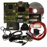
R0K572030S000BE Renesas Electronics America, R0K572030S000BE Datasheet - Page 419

R0K572030S000BE
Manufacturer Part Number
R0K572030S000BE
Description
KIT DEV FOR SH7203
Manufacturer
Renesas Electronics America
Series
Renesas Starter Kits (RSK)r
Type
MCUr
Specifications of R0K572030S000BE
Contents
CPU Board, LCD Module, E10A-Lite Emulator, Cable, QuickStart Guide and CD-ROM
Silicon Manufacturer
Renesas
Kit Contents
Board
Silicon Family Name
SH7203
Silicon Core Number
R5S72030W200FP
Tool / Board Applications
General Purpose MCU, MPU, DSP, DSC
Mcu Supported Families
SH7203
Lead Free Status / RoHS Status
Contains lead / RoHS non-compliant
For Use With/related Products
SH7203
Lead Free Status / Rohs Status
Compliant
- Current page: 419 of 1686
- Download datasheet (10Mb)
9.5.13
The bus arbitration of this LSI has the bus mastership in the normal state and releases the bus
mastership after receiving a bus request from another device.
Bus mastership is transferred at the boundary of bus cycles. Namely, bus mastership is released
immediately after receiving a bus request when a bus cycle is not being performed. The release of
bus mastership is delayed until the bus cycle is complete when a bus cycle is in progress. Even
when from outside the LSI it looks like a bus cycle is not being performed, a bus cycle may be
performing internally, started by inserting wait cycles between access cycles. Therefore, it cannot
be immediately determined whether or not bus mastership has been released by looking at the CSn
signal or other bus control signals. The states that do not allow bus mastership release are shown
below.
1. 16-byte transfer because of a cache miss
2. During write-back operation for the cache
3. Between the read and write cycles of a TAS instruction
4. Multiple bus cycles generated when the data bus width is smaller than the access size (for
5. 16-byte transfer by the DMAC
6. Setting the BLOCK bit in CMNCR to 1
7. 16-byte to 128-byte transfer by the LCDC
Moreover, by using DPRTY bit in CMNCR, whether the bus mastership request is received or not
can be selected during DMAC burst transfer.
The LSI has the bus mastership until a bus request is received from another device. Upon
acknowledging the assertion (low level) of the external bus request signal BREQ, the LSI releases
the bus at the completion of the current bus cycle and asserts the BACK signal. After the LSI
acknowledges the negation (high level) of the BREQ signal that indicates the external device has
released the bus, it negates the BACK signal and resumes the bus usage.
With the SDRAM interface, all bank pre-charge commands (PALLs) are issued when active banks
exist and the bus is released after completion of a PALL command.
The bus sequence is as follows. The address bus and data bus are placed in a high-impedance state
synchronized with the rising edge of CKIO. The bus mastership enable signal is asserted 0.5
cycles after the above timing, synchronized with the falling edge of CKIO. The bus control signals
(BS, CSn, RASU, RASL, CASU, CASL, CKE, DQMxx, WEn, RD, and RD/WR) are placed in
example, between bus cycles when longword access is made to a memory with a data bus
width of 8 bits)
Bus Arbitration
Rev. 3.00 Sep. 28, 2009 Page 387 of 1650
Section 9 Bus State Controller (BSC)
REJ09B0313-0300
Related parts for R0K572030S000BE
Image
Part Number
Description
Manufacturer
Datasheet
Request
R

Part Number:
Description:
KIT STARTER FOR M16C/29
Manufacturer:
Renesas Electronics America
Datasheet:

Part Number:
Description:
KIT STARTER FOR R8C/2D
Manufacturer:
Renesas Electronics America
Datasheet:

Part Number:
Description:
R0K33062P STARTER KIT
Manufacturer:
Renesas Electronics America
Datasheet:

Part Number:
Description:
KIT STARTER FOR R8C/23 E8A
Manufacturer:
Renesas Electronics America
Datasheet:

Part Number:
Description:
KIT STARTER FOR R8C/25
Manufacturer:
Renesas Electronics America
Datasheet:

Part Number:
Description:
KIT STARTER H8S2456 SHARPE DSPLY
Manufacturer:
Renesas Electronics America
Datasheet:

Part Number:
Description:
KIT STARTER FOR R8C38C
Manufacturer:
Renesas Electronics America
Datasheet:

Part Number:
Description:
KIT STARTER FOR R8C35C
Manufacturer:
Renesas Electronics America
Datasheet:

Part Number:
Description:
KIT STARTER FOR R8CL3AC+LCD APPS
Manufacturer:
Renesas Electronics America
Datasheet:

Part Number:
Description:
KIT STARTER FOR RX610
Manufacturer:
Renesas Electronics America
Datasheet:

Part Number:
Description:
KIT STARTER FOR R32C/118
Manufacturer:
Renesas Electronics America
Datasheet:

Part Number:
Description:
KIT DEV RSK-R8C/26-29
Manufacturer:
Renesas Electronics America
Datasheet:

Part Number:
Description:
KIT STARTER FOR SH7124
Manufacturer:
Renesas Electronics America
Datasheet:

Part Number:
Description:
KIT STARTER FOR H8SX/1622
Manufacturer:
Renesas Electronics America
Datasheet:

Part Number:
Description:
KIT STARTER FOR R8C/18191A1B
Manufacturer:
Renesas Electronics America
Datasheet:


