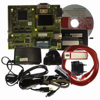
R0K572030S000BE Renesas Electronics America, R0K572030S000BE Datasheet - Page 1477

R0K572030S000BE
Manufacturer Part Number
R0K572030S000BE
Description
KIT DEV FOR SH7203
Manufacturer
Renesas Electronics America
Series
Renesas Starter Kits (RSK)r
Type
MCUr
Specifications of R0K572030S000BE
Contents
CPU Board, LCD Module, E10A-Lite Emulator, Cable, QuickStart Guide and CD-ROM
Silicon Manufacturer
Renesas
Kit Contents
Board
Silicon Family Name
SH7203
Silicon Core Number
R5S72030W200FP
Tool / Board Applications
General Purpose MCU, MPU, DSP, DSC
Mcu Supported Families
SH7203
Lead Free Status / RoHS Status
Contains lead / RoHS non-compliant
For Use With/related Products
SH7203
Lead Free Status / Rohs Status
Compliant
- Current page: 1477 of 1686
- Download datasheet (10Mb)
This section gives information on the on-chip I/O registers of this LSI in the following structures.
1. Register Addresses (by functional module, in order of the corresponding section numbers)
2. Register Bits
3. Register States in Each Operating Mode
4. Notes when Writing to the On-Chip Peripheral Modules
⎯ Registers are described by functional module, in order of the corresponding section
⎯ Access to reserved addresses which are not described in this register address list is
⎯ When registers consist of 16 or 32 bits, the addresses of the MSBs are given when big
⎯ Bit configurations of the registers are described in the same order as the Register Addresses
⎯ Reserved bits are indicated by — in the bit name.
⎯ No entry in the bit-name column indicates that the whole register is allocated as a counter
⎯ Register states are described in the same order as the Register Addresses (by functional
⎯ For the initial state of each bit, refer to the description of the register in the corresponding
⎯ The register states described are for the basic operating modes. If there is a specific reset
⎯ To access an on-chip module register, two or more peripheral module clock (Pφ) cycles are
numbers.
prohibited.
endian mode is selected.
(by functional module, in order of the corresponding section numbers).
or for holding data.
module, in order of the corresponding section numbers).
section.
for an on-chip peripheral module, refer to the section on that on-chip peripheral module.
required. Care must be taken in system design. When the CPU writes data to the internal
peripheral registers, the CPU performs the succeeding instructions without waiting for the
completion of writing to registers. For example, a case is described here in which the
system is transferring to the software standby mode for power savings. To make this
transition, the SLEEP instruction must be performed after setting the STBY bit in the
STBCR register to 1. However a dummy read of the STBCR register is required before
executing the SLEEP instruction. If a dummy read is omitted, the CPU executes the SLEEP
instruction before the STBY bit is set to 1, thus the system enters sleep mode not software
standby mode. A dummy read of the STBCR register is indispensable to complete writing
to the STBY bit. To reflect the change by internal peripheral registers while performing the
succeeding instructions, execute a dummy read of registers to which write instruction is
given and then perform the succeeding instructions.
Section 30 List of Registers
Rev. 3.00 Sep. 28, 2009 Page 1445 of 1650
Section 30 List of Registers
REJ09B0313-0300
Related parts for R0K572030S000BE
Image
Part Number
Description
Manufacturer
Datasheet
Request
R

Part Number:
Description:
KIT STARTER FOR M16C/29
Manufacturer:
Renesas Electronics America
Datasheet:

Part Number:
Description:
KIT STARTER FOR R8C/2D
Manufacturer:
Renesas Electronics America
Datasheet:

Part Number:
Description:
R0K33062P STARTER KIT
Manufacturer:
Renesas Electronics America
Datasheet:

Part Number:
Description:
KIT STARTER FOR R8C/23 E8A
Manufacturer:
Renesas Electronics America
Datasheet:

Part Number:
Description:
KIT STARTER FOR R8C/25
Manufacturer:
Renesas Electronics America
Datasheet:

Part Number:
Description:
KIT STARTER H8S2456 SHARPE DSPLY
Manufacturer:
Renesas Electronics America
Datasheet:

Part Number:
Description:
KIT STARTER FOR R8C38C
Manufacturer:
Renesas Electronics America
Datasheet:

Part Number:
Description:
KIT STARTER FOR R8C35C
Manufacturer:
Renesas Electronics America
Datasheet:

Part Number:
Description:
KIT STARTER FOR R8CL3AC+LCD APPS
Manufacturer:
Renesas Electronics America
Datasheet:

Part Number:
Description:
KIT STARTER FOR RX610
Manufacturer:
Renesas Electronics America
Datasheet:

Part Number:
Description:
KIT STARTER FOR R32C/118
Manufacturer:
Renesas Electronics America
Datasheet:

Part Number:
Description:
KIT DEV RSK-R8C/26-29
Manufacturer:
Renesas Electronics America
Datasheet:

Part Number:
Description:
KIT STARTER FOR SH7124
Manufacturer:
Renesas Electronics America
Datasheet:

Part Number:
Description:
KIT STARTER FOR H8SX/1622
Manufacturer:
Renesas Electronics America
Datasheet:

Part Number:
Description:
KIT STARTER FOR R8C/18191A1B
Manufacturer:
Renesas Electronics America
Datasheet:


