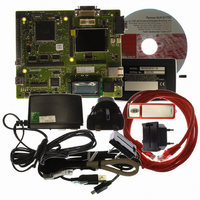
R0K572030S000BE Renesas Electronics America, R0K572030S000BE Datasheet - Page 1655

R0K572030S000BE
Manufacturer Part Number
R0K572030S000BE
Description
KIT DEV FOR SH7203
Manufacturer
Renesas Electronics America
Series
Renesas Starter Kits (RSK)r
Type
MCUr
Specifications of R0K572030S000BE
Contents
CPU Board, LCD Module, E10A-Lite Emulator, Cable, QuickStart Guide and CD-ROM
Silicon Manufacturer
Renesas
Kit Contents
Board
Silicon Family Name
SH7203
Silicon Core Number
R5S72030W200FP
Tool / Board Applications
General Purpose MCU, MPU, DSP, DSC
Mcu Supported Families
SH7203
Lead Free Status / RoHS Status
Contains lead / RoHS non-compliant
For Use With/related Products
SH7203
Lead Free Status / Rohs Status
Compliant
- Current page: 1655 of 1686
- Download datasheet (10Mb)
Item
10.5.1 Setting of the
Half-End Flag and
Generation of the Half-
End Interrupt
10.5.5 Notes on Using
Flag Bits
11.3.2 Timer Mode
Register (TMDR)
11.3.5 Timer Status
Register (TSR)
•
•
TSR_0, TSR_1,
TSR_2, TSR_3,
TSR_4
TSR2_0
Page
444
447
464
490
491
Revision (See Manual for Details)
Description amended
When executing DMA transfer by reload function of DMAC,
setting different value to DMA reload transfer count register
(RDMATCR_n) from the DMA transfer count register
(DMATCR_n) value set when transfer is started lead to an
error in the operation of the half end flag of DMA channel
control register (CHCR_n). Even though the value of
DMATCR_n is rewritten by reload operation, half end flag is
set based on the value set when transfer is started. Because
of this, there may be errors where (a) the set timing of the
half end flag is not correct, or (b) the half end flag can not be
set, may be generated. When executing DMA transfer by
reload function under the condition that different values are
set to RDMATCR_n from DMATCR_n, do not use half end
flag or half end interrupt.
Newly added
Table amended
Notes amended
Notes: 2. If the next flag is set before TGFA is cleared to 0
Notes amended
Notes: 2. If the next flag is set before TGFE is cleared to 0
Bit
5
Bit Name
BFB
after reading TGFA = 1, TGFA remains 1 even
when 0 is written to. In this case, read TGFA = 1
again to clear TGFA to 0.
after reading TGFE = 1, TGFE remains 1 even
when 0 is written to. In this case, read TGFE = 1
again to clear TGFE to 0.
Initial
Value
0
R/W
R/W
Rev. 3.00 Sep. 28, 2009 Page 1623 of 1650
Description
Buffer Operation B
Specifies whether TGRB is to operate in the normal
way, or TGRB and TGRD are to be used together for
buffer operation. When TGRD is used as a buffer
register, TGRD input capture/output compare is not
generated in a mode other than complementary PWM.
In channels 1 and 2, which have no TGRD, bit 5 is
reserved. It is always read as 0 and cannot be modified.
0: TGRB and TGRD operate normally
1: TGRB and TGRD used together for buffer operation
REJ09B0313-0300
Related parts for R0K572030S000BE
Image
Part Number
Description
Manufacturer
Datasheet
Request
R

Part Number:
Description:
KIT STARTER FOR M16C/29
Manufacturer:
Renesas Electronics America
Datasheet:

Part Number:
Description:
KIT STARTER FOR R8C/2D
Manufacturer:
Renesas Electronics America
Datasheet:

Part Number:
Description:
R0K33062P STARTER KIT
Manufacturer:
Renesas Electronics America
Datasheet:

Part Number:
Description:
KIT STARTER FOR R8C/23 E8A
Manufacturer:
Renesas Electronics America
Datasheet:

Part Number:
Description:
KIT STARTER FOR R8C/25
Manufacturer:
Renesas Electronics America
Datasheet:

Part Number:
Description:
KIT STARTER H8S2456 SHARPE DSPLY
Manufacturer:
Renesas Electronics America
Datasheet:

Part Number:
Description:
KIT STARTER FOR R8C38C
Manufacturer:
Renesas Electronics America
Datasheet:

Part Number:
Description:
KIT STARTER FOR R8C35C
Manufacturer:
Renesas Electronics America
Datasheet:

Part Number:
Description:
KIT STARTER FOR R8CL3AC+LCD APPS
Manufacturer:
Renesas Electronics America
Datasheet:

Part Number:
Description:
KIT STARTER FOR RX610
Manufacturer:
Renesas Electronics America
Datasheet:

Part Number:
Description:
KIT STARTER FOR R32C/118
Manufacturer:
Renesas Electronics America
Datasheet:

Part Number:
Description:
KIT DEV RSK-R8C/26-29
Manufacturer:
Renesas Electronics America
Datasheet:

Part Number:
Description:
KIT STARTER FOR SH7124
Manufacturer:
Renesas Electronics America
Datasheet:

Part Number:
Description:
KIT STARTER FOR H8SX/1622
Manufacturer:
Renesas Electronics America
Datasheet:

Part Number:
Description:
KIT STARTER FOR R8C/18191A1B
Manufacturer:
Renesas Electronics America
Datasheet:


