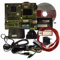
R0K572030S000BE Renesas Electronics America, R0K572030S000BE Datasheet - Page 372

R0K572030S000BE
Manufacturer Part Number
R0K572030S000BE
Description
KIT DEV FOR SH7203
Manufacturer
Renesas Electronics America
Series
Renesas Starter Kits (RSK)r
Type
MCUr
Specifications of R0K572030S000BE
Contents
CPU Board, LCD Module, E10A-Lite Emulator, Cable, QuickStart Guide and CD-ROM
Silicon Manufacturer
Renesas
Kit Contents
Board
Silicon Family Name
SH7203
Silicon Core Number
R5S72030W200FP
Tool / Board Applications
General Purpose MCU, MPU, DSP, DSC
Mcu Supported Families
SH7203
Lead Free Status / RoHS Status
Contains lead / RoHS non-compliant
For Use With/related Products
SH7203
Lead Free Status / Rohs Status
Compliant
- Current page: 372 of 1686
- Download datasheet (10Mb)
Section 9 Bus State Controller (BSC)
(7)
Bank Active
The SDRAM bank function can be used to support high-speed access to the same row address.
When the BACTV bit in SDCR is 1, access is performed using commands without auto-precharge
(READ or WRIT). This function is called bank-active function. This function is valid only for
either the upper or lower bits of area 3. When area 3 is set to bank-active mode, area 2 should be
set to normal space or SRAM with byte selection. When areas 2 and 3 are both set to SDRAM or
both the upper and lower bits of area 3 are connected to SDRAM, auto precharge mode must be
set.
When the bank-active function is used, precharging is not performed when the access ends. When
accessing the same row address in the same bank, it is possible to issue the READ or WRIT
command immediately, without issuing an ACTV command. As SDRAM is internally divided
into several banks, it is possible to activate one row address in each bank. If the next access is to a
different row address, a PRE command is first issued to precharge the relevant bank, then when
precharging is completed, the access is performed by issuing an ACTV command followed by a
READ or WRIT command. If this is followed by an access to a different row address, the access
time will be longer because of the precharging performed after the access request is issued. The
number of cycles between issuance of the PRE command and the ACTV command is determined
by the WTRP1 and WTPR0 bits in CS3WCR.
In a write, when an auto-precharge is performed, a command cannot be issued to the same bank
for a period of Trwl + Tap cycles after issuance of the WRITA command. When bank active mode
is used, READ or WRIT commands can be issued successively if the row address is the same. The
number of cycles can thus be reduced by Trwl + Tap cycles for each write.
There is a limit on tRAS, the time for placing each bank in the active state. If there is no guarantee
that there will not be a cache hit and another row address will be accessed within the period in
which this value is maintained by program execution, it is necessary to set auto-refresh and set the
refresh cycle to no more than the maximum value of tRAS.
A burst read cycle without auto-precharge is shown in figure 9.22, a burst read cycle for the same
row address in figure 9.23, and a burst read cycle for different row addresses in figure 9.24.
Similarly, a burst write cycle without auto-precharge is shown in figure 9.25, a burst write cycle
for the same row address in figure 9.26, and a burst write cycle for different row addresses in
figure 9.27.
In figure 9.23, a Tnop cycle in which no operation is performed is inserted before the Tc cycle that
issues the READ command. The Tnop cycle is inserted to acquire two cycles of CAS latency for
the DQMxx signal that specifies the read byte in the data read from the SDRAM. If the CAS
Rev. 3.00 Sep. 28, 2009 Page 340 of 1650
REJ09B0313-0300
Related parts for R0K572030S000BE
Image
Part Number
Description
Manufacturer
Datasheet
Request
R

Part Number:
Description:
KIT STARTER FOR M16C/29
Manufacturer:
Renesas Electronics America
Datasheet:

Part Number:
Description:
KIT STARTER FOR R8C/2D
Manufacturer:
Renesas Electronics America
Datasheet:

Part Number:
Description:
R0K33062P STARTER KIT
Manufacturer:
Renesas Electronics America
Datasheet:

Part Number:
Description:
KIT STARTER FOR R8C/23 E8A
Manufacturer:
Renesas Electronics America
Datasheet:

Part Number:
Description:
KIT STARTER FOR R8C/25
Manufacturer:
Renesas Electronics America
Datasheet:

Part Number:
Description:
KIT STARTER H8S2456 SHARPE DSPLY
Manufacturer:
Renesas Electronics America
Datasheet:

Part Number:
Description:
KIT STARTER FOR R8C38C
Manufacturer:
Renesas Electronics America
Datasheet:

Part Number:
Description:
KIT STARTER FOR R8C35C
Manufacturer:
Renesas Electronics America
Datasheet:

Part Number:
Description:
KIT STARTER FOR R8CL3AC+LCD APPS
Manufacturer:
Renesas Electronics America
Datasheet:

Part Number:
Description:
KIT STARTER FOR RX610
Manufacturer:
Renesas Electronics America
Datasheet:

Part Number:
Description:
KIT STARTER FOR R32C/118
Manufacturer:
Renesas Electronics America
Datasheet:

Part Number:
Description:
KIT DEV RSK-R8C/26-29
Manufacturer:
Renesas Electronics America
Datasheet:

Part Number:
Description:
KIT STARTER FOR SH7124
Manufacturer:
Renesas Electronics America
Datasheet:

Part Number:
Description:
KIT STARTER FOR H8SX/1622
Manufacturer:
Renesas Electronics America
Datasheet:

Part Number:
Description:
KIT STARTER FOR R8C/18191A1B
Manufacturer:
Renesas Electronics America
Datasheet:


