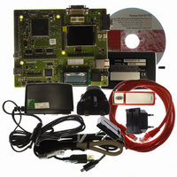
R0K572030S000BE Renesas Electronics America, R0K572030S000BE Datasheet - Page 801

R0K572030S000BE
Manufacturer Part Number
R0K572030S000BE
Description
KIT DEV FOR SH7203
Manufacturer
Renesas Electronics America
Series
Renesas Starter Kits (RSK)r
Type
MCUr
Specifications of R0K572030S000BE
Contents
CPU Board, LCD Module, E10A-Lite Emulator, Cable, QuickStart Guide and CD-ROM
Silicon Manufacturer
Renesas
Kit Contents
Board
Silicon Family Name
SH7203
Silicon Core Number
R5S72030W200FP
Tool / Board Applications
General Purpose MCU, MPU, DSP, DSC
Mcu Supported Families
SH7203
Lead Free Status / RoHS Status
Contains lead / RoHS non-compliant
For Use With/related Products
SH7203
Lead Free Status / Rohs Status
Compliant
- Current page: 801 of 1686
- Download datasheet (10Mb)
Figure 15.3 shows a sample flowchart for initializing the SCIF.
After reading flags ER, DR, and BRK in SCFSR,
(leaving bits TIE, RIE, TE, and RE cleared to 0)
Set the RTRG1, RTRG0, TTRG1, TTRG0, and
and each flag in SCLSR, write 0 to clear them
Set the TFRST and RFRST bits in SCFCR to 1
Set the BGDM and ABCS bits in SCEMR
Set the CKE1 and CKE0 bits in SCSCR
Clear the TE and RE bits in SCSCR to 0
Set the TE and RE bits in SCSCR to 1,
Set data transfer format in SCSMR
and set the TIE, RIE, and REIE bits
clear TFRST and RFRST bits to 0
PFC setting for external pins used
MCE bits in SCFCR, and
Figure 15.3 Sample Flowchart for SCIF Initialization
Set value in SCBRR
Start of initialization
End of initialization
SCK, TxD, RxD
Section 15 Serial Communication Interface with FIFO (SCIF)
[1]
[2]
[3]
[4]
[5]
[1]
[2]
[3]
[4]
[5]
Set the clock selection in SCSCR.
Be sure to clear bits TIE, RIE, TE,
and RE to 0.
Set the data transfer format in
SCSMR.
Write a value corresponding to the
bit rate into SCBRR. (Not
necessary if an external clock is
used.)
Sets PFC for external pins used.
Set as RxD input at receiving and
TxD at transmission.
However, no setting for SCK pin is
required when CKE[1:0] is 00.
In the case when internal synchronous
clock output is set, the SCK pin starts
outputting the clock at this stage.
Set the TE bit or RE bit in SCSCR
to 1. Also set the RIE, REIE, and
TIE bits. Setting the TE and RE bits
enables the TxD and RxD pins to be
used.
When transmitting, the SCIF will go
to the mark state; when receiving,
it will go to the idle state, waiting for
a start bit.
Rev. 3.00 Sep. 28, 2009 Page 769 of 1650
REJ09B0313-0300
Related parts for R0K572030S000BE
Image
Part Number
Description
Manufacturer
Datasheet
Request
R

Part Number:
Description:
KIT STARTER FOR M16C/29
Manufacturer:
Renesas Electronics America
Datasheet:

Part Number:
Description:
KIT STARTER FOR R8C/2D
Manufacturer:
Renesas Electronics America
Datasheet:

Part Number:
Description:
R0K33062P STARTER KIT
Manufacturer:
Renesas Electronics America
Datasheet:

Part Number:
Description:
KIT STARTER FOR R8C/23 E8A
Manufacturer:
Renesas Electronics America
Datasheet:

Part Number:
Description:
KIT STARTER FOR R8C/25
Manufacturer:
Renesas Electronics America
Datasheet:

Part Number:
Description:
KIT STARTER H8S2456 SHARPE DSPLY
Manufacturer:
Renesas Electronics America
Datasheet:

Part Number:
Description:
KIT STARTER FOR R8C38C
Manufacturer:
Renesas Electronics America
Datasheet:

Part Number:
Description:
KIT STARTER FOR R8C35C
Manufacturer:
Renesas Electronics America
Datasheet:

Part Number:
Description:
KIT STARTER FOR R8CL3AC+LCD APPS
Manufacturer:
Renesas Electronics America
Datasheet:

Part Number:
Description:
KIT STARTER FOR RX610
Manufacturer:
Renesas Electronics America
Datasheet:

Part Number:
Description:
KIT STARTER FOR R32C/118
Manufacturer:
Renesas Electronics America
Datasheet:

Part Number:
Description:
KIT DEV RSK-R8C/26-29
Manufacturer:
Renesas Electronics America
Datasheet:

Part Number:
Description:
KIT STARTER FOR SH7124
Manufacturer:
Renesas Electronics America
Datasheet:

Part Number:
Description:
KIT STARTER FOR H8SX/1622
Manufacturer:
Renesas Electronics America
Datasheet:

Part Number:
Description:
KIT STARTER FOR R8C/18191A1B
Manufacturer:
Renesas Electronics America
Datasheet:


