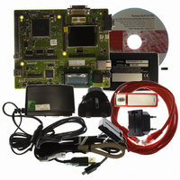
R0K572030S000BE Renesas Electronics America, R0K572030S000BE Datasheet - Page 1065

R0K572030S000BE
Manufacturer Part Number
R0K572030S000BE
Description
KIT DEV FOR SH7203
Manufacturer
Renesas Electronics America
Series
Renesas Starter Kits (RSK)r
Type
MCUr
Specifications of R0K572030S000BE
Contents
CPU Board, LCD Module, E10A-Lite Emulator, Cable, QuickStart Guide and CD-ROM
Silicon Manufacturer
Renesas
Kit Contents
Board
Silicon Family Name
SH7203
Silicon Core Number
R5S72030W200FP
Tool / Board Applications
General Purpose MCU, MPU, DSP, DSC
Mcu Supported Families
SH7203
Lead Free Status / RoHS Status
Contains lead / RoHS non-compliant
For Use With/related Products
SH7203
Lead Free Status / Rohs Status
Compliant
- Current page: 1065 of 1686
- Download datasheet (10Mb)
20.4.3
Scan mode is useful for monitoring analog inputs in a group of one or more channels at all times.
In scan mode, A/D conversion is performed sequentially for a maximum of eight specified analog
input channels, as follows:
1. A/D conversion starts from the analog input channel with the lowest number (e.g. AN0, AN1,
2. When A/D conversion is completed on each channel, the A/D conversion result is sequentially
3. After A/D conversion on all selected channels has completed, the ADF bit in ADCSR is set to
4. The ADST bit is not cleared automatically, so steps 2. and 3. are repeated as long as the ADST
When the operating mode or analog input channel selection must be changed during A/D
conversion, to prevent incorrect operation, first clear the ADST bit to 0 to halt A/D conversion.
After making the necessary changes, set the ADST bit to 1. A/D conversion will start again from
the first channel in the group. The ADST bit can be set at the same time as the mode or channel
selection is changed.
Typical operations when three channels (AN0 to AN2) are selected in scan mode are described as
follows. Figure 20.4 shows a timing diagram for this example.
1. Scan mode is selected (MDS2 = 1, MDS1 = 1), analog input channels AN0 to AN2 are
2. A/D conversion of the first channel (AN0) starts. When A/D conversion is completed, the A/D
3. Next, the second channel (AN1) is selected automatically and A/D conversion starts.
4. Conversion proceeds in the same way through the third channel (AN2).
5. When conversion of all the selected channels (AN0 to AN2) is completed, the ADF flag is set
…, AN3) when the ADST bit in ADCSR is set to 1 by software, MTU2, or external trigger
input.
transferred to the A/D data register corresponding to that channel.
1. If the ADIE bit is set to 1 at this time, an ADI interrupt request is generated. The A/D
converter starts A/D conversion again from the channel with the lowest number.
bit remains set to 1. When the ADST bit is cleared to 0, A/D conversion halts and the A/D
converter becomes idle.
The ADF bit is cleared by reading ADF while ADF = 1, then writing 0 to the ADF bit.
selected (CH[2:0] = 010), and A/D conversion is started (ADST = 1).
conversion result is transferred into ADDRA.
to 1 and conversion of the first channel (AN0) starts again. If the ADIE bit is set to 1 at this
time, an ADI interrupt is requested.
Scan Mode
Rev. 3.00 Sep. 28, 2009 Page 1033 of 1650
Section 20 A/D Converter (ADC)
REJ09B0313-0300
Related parts for R0K572030S000BE
Image
Part Number
Description
Manufacturer
Datasheet
Request
R

Part Number:
Description:
KIT STARTER FOR M16C/29
Manufacturer:
Renesas Electronics America
Datasheet:

Part Number:
Description:
KIT STARTER FOR R8C/2D
Manufacturer:
Renesas Electronics America
Datasheet:

Part Number:
Description:
R0K33062P STARTER KIT
Manufacturer:
Renesas Electronics America
Datasheet:

Part Number:
Description:
KIT STARTER FOR R8C/23 E8A
Manufacturer:
Renesas Electronics America
Datasheet:

Part Number:
Description:
KIT STARTER FOR R8C/25
Manufacturer:
Renesas Electronics America
Datasheet:

Part Number:
Description:
KIT STARTER H8S2456 SHARPE DSPLY
Manufacturer:
Renesas Electronics America
Datasheet:

Part Number:
Description:
KIT STARTER FOR R8C38C
Manufacturer:
Renesas Electronics America
Datasheet:

Part Number:
Description:
KIT STARTER FOR R8C35C
Manufacturer:
Renesas Electronics America
Datasheet:

Part Number:
Description:
KIT STARTER FOR R8CL3AC+LCD APPS
Manufacturer:
Renesas Electronics America
Datasheet:

Part Number:
Description:
KIT STARTER FOR RX610
Manufacturer:
Renesas Electronics America
Datasheet:

Part Number:
Description:
KIT STARTER FOR R32C/118
Manufacturer:
Renesas Electronics America
Datasheet:

Part Number:
Description:
KIT DEV RSK-R8C/26-29
Manufacturer:
Renesas Electronics America
Datasheet:

Part Number:
Description:
KIT STARTER FOR SH7124
Manufacturer:
Renesas Electronics America
Datasheet:

Part Number:
Description:
KIT STARTER FOR H8SX/1622
Manufacturer:
Renesas Electronics America
Datasheet:

Part Number:
Description:
KIT STARTER FOR R8C/18191A1B
Manufacturer:
Renesas Electronics America
Datasheet:


