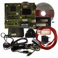
R0K572030S000BE Renesas Electronics America, R0K572030S000BE Datasheet - Page 329

R0K572030S000BE
Manufacturer Part Number
R0K572030S000BE
Description
KIT DEV FOR SH7203
Manufacturer
Renesas Electronics America
Series
Renesas Starter Kits (RSK)r
Type
MCUr
Specifications of R0K572030S000BE
Contents
CPU Board, LCD Module, E10A-Lite Emulator, Cable, QuickStart Guide and CD-ROM
Silicon Manufacturer
Renesas
Kit Contents
Board
Silicon Family Name
SH7203
Silicon Core Number
R5S72030W200FP
Tool / Board Applications
General Purpose MCU, MPU, DSP, DSC
Mcu Supported Families
SH7203
Lead Free Status / RoHS Status
Contains lead / RoHS non-compliant
For Use With/related Products
SH7203
Lead Free Status / Rohs Status
Compliant
- Current page: 329 of 1686
- Download datasheet (10Mb)
9.5
9.5.1
This LSI supports both big endian, in which the most significant byte (MSB) of data is that in the
direction of the 0th address, and little endian, in which the least significant byte (LSB) is that in
the direction of the 0th address. In the initial state after a power-on reset, all areas will be in big
endian mode. Little endian cannot be selected for area 0. However, the endian of areas 1 to 7 can
be changed by the setting in the CSnBCR register setting as long as the target space is not being
accessed.
Three data bus widths (8 bits, 16 bits, and 32 bits) are selectable for areas 1 to 7, allowing the
connection of normal memory and of SRAM with byte selection. Two data bus widths (16 bits and
32 bits) are available for SDRAM. Two data bus widths (8 bits and 16 bits) are available for the
PCMCIA interface. For MPX-I/O, the data bus width can be fixed to either 8 or 16 bits, or made
selectable as 8 bits or 16 bits by one of the address lines. The data bus width for burst MPX-I/O is
fixed at 32 bits. Data alignment is in accord with the data bus width selected for the device. This
also means that four read operations are required to read longword data from a byte-width device.
In this LSI, data alignment and conversion of data length is performed automatically between the
respective interfaces. The data bus width of area 0 is fixed to 16 bits or 32 bits by the MD pin
setting at a power-on reset.
Tables 9.5 to 9.10 show the relationship between device data width and access unit. Note that the
correspondence between addresses and strobe signals for the 32- and 16-bit bus widths depends on
the endian setting. For example, with big endian and a 32-bit bus width, WE3 corresponds to the
0th address, which is represented by WE0 when little endian has been selected. Area 0 cannot be
set to little endian mode. In addition, fetching instructions from a little endian area can be difficult
because 32-bit and 16-bit accesses are mixed, so big endian mode should be used for instruction
execution.
Operation
Endian/Access Size and Data Alignment
Rev. 3.00 Sep. 28, 2009 Page 297 of 1650
Section 9 Bus State Controller (BSC)
REJ09B0313-0300
Related parts for R0K572030S000BE
Image
Part Number
Description
Manufacturer
Datasheet
Request
R

Part Number:
Description:
KIT STARTER FOR M16C/29
Manufacturer:
Renesas Electronics America
Datasheet:

Part Number:
Description:
KIT STARTER FOR R8C/2D
Manufacturer:
Renesas Electronics America
Datasheet:

Part Number:
Description:
R0K33062P STARTER KIT
Manufacturer:
Renesas Electronics America
Datasheet:

Part Number:
Description:
KIT STARTER FOR R8C/23 E8A
Manufacturer:
Renesas Electronics America
Datasheet:

Part Number:
Description:
KIT STARTER FOR R8C/25
Manufacturer:
Renesas Electronics America
Datasheet:

Part Number:
Description:
KIT STARTER H8S2456 SHARPE DSPLY
Manufacturer:
Renesas Electronics America
Datasheet:

Part Number:
Description:
KIT STARTER FOR R8C38C
Manufacturer:
Renesas Electronics America
Datasheet:

Part Number:
Description:
KIT STARTER FOR R8C35C
Manufacturer:
Renesas Electronics America
Datasheet:

Part Number:
Description:
KIT STARTER FOR R8CL3AC+LCD APPS
Manufacturer:
Renesas Electronics America
Datasheet:

Part Number:
Description:
KIT STARTER FOR RX610
Manufacturer:
Renesas Electronics America
Datasheet:

Part Number:
Description:
KIT STARTER FOR R32C/118
Manufacturer:
Renesas Electronics America
Datasheet:

Part Number:
Description:
KIT DEV RSK-R8C/26-29
Manufacturer:
Renesas Electronics America
Datasheet:

Part Number:
Description:
KIT STARTER FOR SH7124
Manufacturer:
Renesas Electronics America
Datasheet:

Part Number:
Description:
KIT STARTER FOR H8SX/1622
Manufacturer:
Renesas Electronics America
Datasheet:

Part Number:
Description:
KIT STARTER FOR R8C/18191A1B
Manufacturer:
Renesas Electronics America
Datasheet:


