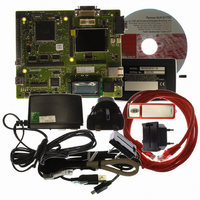
R0K572030S000BE Renesas Electronics America, R0K572030S000BE Datasheet - Page 819

R0K572030S000BE
Manufacturer Part Number
R0K572030S000BE
Description
KIT DEV FOR SH7203
Manufacturer
Renesas Electronics America
Series
Renesas Starter Kits (RSK)r
Type
MCUr
Specifications of R0K572030S000BE
Contents
CPU Board, LCD Module, E10A-Lite Emulator, Cable, QuickStart Guide and CD-ROM
Silicon Manufacturer
Renesas
Kit Contents
Board
Silicon Family Name
SH7203
Silicon Core Number
R5S72030W200FP
Tool / Board Applications
General Purpose MCU, MPU, DSP, DSC
Mcu Supported Families
SH7203
Lead Free Status / RoHS Status
Contains lead / RoHS non-compliant
For Use With/related Products
SH7203
Lead Free Status / Rohs Status
Compliant
- Current page: 819 of 1686
- Download datasheet (10Mb)
15.6.3
When the DMAC writes data to SCFTDR due to a TXI interrupt request, the state of the TEND
flag becomes undefined. Therefore, the TEND flag should not be used as the transfer end flag in
such a case.
15.6.4
Break signals can be detected by reading the RxD pin directly when a framing error (FER) is
detected. In the break state the input from the RxD pin consists of all 0s, so the FER flag is set and
the parity error flag (PER) may also be set.
Note that, although transfer of receive data to SCFRDR is halted in the break state, the SCIF
receiver continues to operate.
15.6.5
The I/O condition and level of the TxD pin are determined by the SPB2IO and SPB2DT bits in the
serial port register (SCSPTR). This feature can be used to send a break signal.
Until TE bit is set to 1 (enabling transmission) after initializing, the TxD pin does not work.
During the period, mark status is performed by the SPB2DT bit. Therefore, the SPB2IO and
SPB2DT bits should be set to 1 (high level output).
To send a break signal during serial transmission, clear the SPB2DT bit to 0 (designating low
level), then clear the TE bit to 0 (halting transmission). When the TE bit is cleared to 0, the
transmitter is initialized regardless of the current transmission state, and 0 is output from the TxD
pin.
15.6.6
The SCIF operates on a base clock with a frequency 16 or 8 times the bit rate. In reception, the
SCIF synchronizes internally with the fall of the start bit, which it samples on the base clock.
Receive data is latched at the rising edge of the eighth or fourth base clock pulse. When the SCIF
operates on a base clock with a frequency 16 times the bit rate, the receive data is sampled at the
timing shown in figure 15.19.
Restriction on DMAC Usage
Break Detection and Processing
Sending a Break Signal
Receive Data Sampling Timing and Receive Margin (Asynchronous Mode)
Section 15 Serial Communication Interface with FIFO (SCIF)
Rev. 3.00 Sep. 28, 2009 Page 787 of 1650
REJ09B0313-0300
Related parts for R0K572030S000BE
Image
Part Number
Description
Manufacturer
Datasheet
Request
R

Part Number:
Description:
KIT STARTER FOR M16C/29
Manufacturer:
Renesas Electronics America
Datasheet:

Part Number:
Description:
KIT STARTER FOR R8C/2D
Manufacturer:
Renesas Electronics America
Datasheet:

Part Number:
Description:
R0K33062P STARTER KIT
Manufacturer:
Renesas Electronics America
Datasheet:

Part Number:
Description:
KIT STARTER FOR R8C/23 E8A
Manufacturer:
Renesas Electronics America
Datasheet:

Part Number:
Description:
KIT STARTER FOR R8C/25
Manufacturer:
Renesas Electronics America
Datasheet:

Part Number:
Description:
KIT STARTER H8S2456 SHARPE DSPLY
Manufacturer:
Renesas Electronics America
Datasheet:

Part Number:
Description:
KIT STARTER FOR R8C38C
Manufacturer:
Renesas Electronics America
Datasheet:

Part Number:
Description:
KIT STARTER FOR R8C35C
Manufacturer:
Renesas Electronics America
Datasheet:

Part Number:
Description:
KIT STARTER FOR R8CL3AC+LCD APPS
Manufacturer:
Renesas Electronics America
Datasheet:

Part Number:
Description:
KIT STARTER FOR RX610
Manufacturer:
Renesas Electronics America
Datasheet:

Part Number:
Description:
KIT STARTER FOR R32C/118
Manufacturer:
Renesas Electronics America
Datasheet:

Part Number:
Description:
KIT DEV RSK-R8C/26-29
Manufacturer:
Renesas Electronics America
Datasheet:

Part Number:
Description:
KIT STARTER FOR SH7124
Manufacturer:
Renesas Electronics America
Datasheet:

Part Number:
Description:
KIT STARTER FOR H8SX/1622
Manufacturer:
Renesas Electronics America
Datasheet:

Part Number:
Description:
KIT STARTER FOR R8C/18191A1B
Manufacturer:
Renesas Electronics America
Datasheet:


