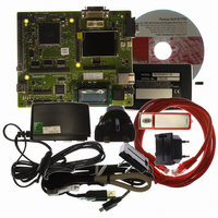
R0K572030S000BE Renesas Electronics America, R0K572030S000BE Datasheet - Page 813

R0K572030S000BE
Manufacturer Part Number
R0K572030S000BE
Description
KIT DEV FOR SH7203
Manufacturer
Renesas Electronics America
Series
Renesas Starter Kits (RSK)r
Type
MCUr
Specifications of R0K572030S000BE
Contents
CPU Board, LCD Module, E10A-Lite Emulator, Cable, QuickStart Guide and CD-ROM
Silicon Manufacturer
Renesas
Kit Contents
Board
Silicon Family Name
SH7203
Silicon Core Number
R5S72030W200FP
Tool / Board Applications
General Purpose MCU, MPU, DSP, DSC
Mcu Supported Families
SH7203
Lead Free Status / RoHS Status
Contains lead / RoHS non-compliant
For Use With/related Products
SH7203
Lead Free Status / Rohs Status
Compliant
- Current page: 813 of 1686
- Download datasheet (10Mb)
In serial transmission, the SCIF operates as described below.
1. When data is written into the transmit FIFO data register (SCFTDR), the SCIF transfers the
2. When data is transferred from SCFTDR to SCTSR and transmission is started, consecutive
3. The SCIF checks the SCFTDR transmit data at the timing for sending the MSB (bit 7). If data
4. After the end of serial transmission, the SCK pin is held in the high state.
Figure 15.14 shows an example of SCIF transmit operation.
data from SCFTDR to the transmit shift register (SCTSR) and starts transmitting. Confirm that
the TDFE flag in the serial status register (SCFSR) is set to 1 before writing transmit data to
SCFTDR. The number of data bytes that can be written is (16 – transmit trigger setting).
transmit operations are performed until there is no transmit data left in SCFTDR. When the
number of transmit data bytes in SCFTDR falls below the transmit trigger number set in the
FIFO control register (SCFCR), the TDFE flag is set. If the TIE bit in the serial control register
(SCSR) is set to 1 at this time, a transmit-FIFO-data-empty interrupt (TXI) request is
generated.
If clock output mode is selected, the SCIF outputs eight synchronous clock pulses. If an
external clock source is selected, the SCIF outputs data in synchronization with the input
clock. Data is output from the TxD pin in order from the LSB (bit 0) to the MSB (bit 7).
is present, the data is transferred from SCFTDR to SCTSR, and then serial transmission of the
next frame is started. If there is no data, the TxD pin holds the state after the TEND flag in
SCFSR is set to 1 and the MSB (bit 7) is sent.
Serial clock
Serial data
TEND
TDFE
interrupt
request
Figure 15.14 Example of SCIF Transmit Operation
TXI
Data written to SCFTDR
Bit 0
LSB
and TDFE flag cleared
to 0 by TXI interrupt
handler
Bit 1
One frame
Section 15 Serial Communication Interface with FIFO (SCIF)
interrupt
request
MSB
Bit 7
TXI
Bit 0
Rev. 3.00 Sep. 28, 2009 Page 781 of 1650
Bit 1
Bit 6
Bit 7
REJ09B0313-0300
Related parts for R0K572030S000BE
Image
Part Number
Description
Manufacturer
Datasheet
Request
R

Part Number:
Description:
KIT STARTER FOR M16C/29
Manufacturer:
Renesas Electronics America
Datasheet:

Part Number:
Description:
KIT STARTER FOR R8C/2D
Manufacturer:
Renesas Electronics America
Datasheet:

Part Number:
Description:
R0K33062P STARTER KIT
Manufacturer:
Renesas Electronics America
Datasheet:

Part Number:
Description:
KIT STARTER FOR R8C/23 E8A
Manufacturer:
Renesas Electronics America
Datasheet:

Part Number:
Description:
KIT STARTER FOR R8C/25
Manufacturer:
Renesas Electronics America
Datasheet:

Part Number:
Description:
KIT STARTER H8S2456 SHARPE DSPLY
Manufacturer:
Renesas Electronics America
Datasheet:

Part Number:
Description:
KIT STARTER FOR R8C38C
Manufacturer:
Renesas Electronics America
Datasheet:

Part Number:
Description:
KIT STARTER FOR R8C35C
Manufacturer:
Renesas Electronics America
Datasheet:

Part Number:
Description:
KIT STARTER FOR R8CL3AC+LCD APPS
Manufacturer:
Renesas Electronics America
Datasheet:

Part Number:
Description:
KIT STARTER FOR RX610
Manufacturer:
Renesas Electronics America
Datasheet:

Part Number:
Description:
KIT STARTER FOR R32C/118
Manufacturer:
Renesas Electronics America
Datasheet:

Part Number:
Description:
KIT DEV RSK-R8C/26-29
Manufacturer:
Renesas Electronics America
Datasheet:

Part Number:
Description:
KIT STARTER FOR SH7124
Manufacturer:
Renesas Electronics America
Datasheet:

Part Number:
Description:
KIT STARTER FOR H8SX/1622
Manufacturer:
Renesas Electronics America
Datasheet:

Part Number:
Description:
KIT STARTER FOR R8C/18191A1B
Manufacturer:
Renesas Electronics America
Datasheet:


