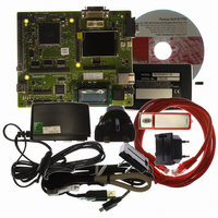
R0K572030S000BE Renesas Electronics America, R0K572030S000BE Datasheet - Page 590

R0K572030S000BE
Manufacturer Part Number
R0K572030S000BE
Description
KIT DEV FOR SH7203
Manufacturer
Renesas Electronics America
Series
Renesas Starter Kits (RSK)r
Type
MCUr
Specifications of R0K572030S000BE
Contents
CPU Board, LCD Module, E10A-Lite Emulator, Cable, QuickStart Guide and CD-ROM
Silicon Manufacturer
Renesas
Kit Contents
Board
Silicon Family Name
SH7203
Silicon Core Number
R5S72030W200FP
Tool / Board Applications
General Purpose MCU, MPU, DSP, DSC
Mcu Supported Families
SH7203
Lead Free Status / RoHS Status
Contains lead / RoHS non-compliant
For Use With/related Products
SH7203
Lead Free Status / Rohs Status
Compliant
- Current page: 590 of 1686
- Download datasheet (10Mb)
Section 11 Multi-Function Timer Pulse Unit 2 (MTU2)
(1)
An example of the complementary PWM mode setting procedure is shown in figure 11.38.
Rev. 3.00 Sep. 28, 2009 Page 558 of 1650
REJ09B0313-0300
Example of Complementary PWM Mode Setting Procedure
Figure 11.38 Example of Complementary PWM Mode Setting Procedure
<Complementary PWM mode>
Inter-channel synchronization
Complementary PWM mode
Complementary PWM mode
Brushless DC motor control
PWM cycle output enabling,
Counter clock, counter clear
Enable/disable dead time
PWM output level setting
Enable waveform output
Dead time, carrier cycle
Stop count operation
Start count operation
Start count operation
source selection
TCNT setting
TGR setting
PFC setting
generation
setting
setting
setting
setting
[1]
[2]
[3]
[4]
[5]
[6]
[7]
[8]
[9]
[10]
[11]
[12]
[13]
[1] Clear bits CST3 and CST4 in the timer start register
[2] Set the same counter clock and clock edge for channels
[3] When performing brushless DC motor control, set bit BDC
[4] Set the dead time in TCNT_3. Set TCNT_4 to H'0000.
[5] Set only when restarting by a synchronous clear from
[6] Set the output PWM duty in the duty registers (TGRB_3,
[7] This setting is necessary only when no dead time should be
[8] Set the dead time in the dead time register (TDDR), 1/2 the
[9] Select enabling/disabling of toggle output synchronized with
[10] Select complementary PWM mode in timer mode register 3
[11] Set enabling/disabling of PWM waveform output pin output in
[12] Set the port control register and the port I/O register.
[13] Set bits CST3 and CST4 in TSTR to 1 simultaneously to start
(TSTR) to 0, and halt timer counter (TCNT) operation.
Perform complementary PWM mode setting when
TCNT_3 and TCNT_4 are stopped.
3 and 4 with bits TPSC2-TPSC0 and bits CKEG1 and
CKEG0 in the timer control register (TCR). Use bits
CCLR2-CCLR0 to set synchronous clearing only when
restarting by a synchronous clear from another channel
during complementary PWM mode operation.
in the timer gate control register (TGCR) and set the
feedback signal input source and output chopping or gate
signal direct output.
another channel during complementary PWM mode
operation. In this case, synchronize the channel generating
the synchronous clear with channels 3 and 4 using the timer
synchro register (TSYR).
TGRA_4, TGRB_4) and buffer registers (TGRD_3, TGRC_4,
TGRD_4). Set the same initial value in each corresponding
TGR.
generated. Make appropriate settings in the timer dead time
enable register (TDER) so that no dead time is generated.
carrier cycle in the carrier cycle data register (TCDR) and
carrier cycle buffer register (TCBR), and 1/2 the carrier cycle
plus the dead time in TGRA_3 and TGRC_3. When no dead
time generation is selected, set 1 in TDDR and 1/2 the carrier
cycle + 1 in TGRA_3 and TGRC_3.
the PWM cycle using bit PSYE in the timer output control
register 1 (TOCR1), and set the PWM output level with bits OLSP
and OLSN. When specifying the PWM output level by using
TOLBR as a buffer for TOCR_2, see figure 11.3.
(TMDR_3). Do not set in TMDR_4.
the timer output master enable register (TOER).
the count operation.
Related parts for R0K572030S000BE
Image
Part Number
Description
Manufacturer
Datasheet
Request
R

Part Number:
Description:
KIT STARTER FOR M16C/29
Manufacturer:
Renesas Electronics America
Datasheet:

Part Number:
Description:
KIT STARTER FOR R8C/2D
Manufacturer:
Renesas Electronics America
Datasheet:

Part Number:
Description:
R0K33062P STARTER KIT
Manufacturer:
Renesas Electronics America
Datasheet:

Part Number:
Description:
KIT STARTER FOR R8C/23 E8A
Manufacturer:
Renesas Electronics America
Datasheet:

Part Number:
Description:
KIT STARTER FOR R8C/25
Manufacturer:
Renesas Electronics America
Datasheet:

Part Number:
Description:
KIT STARTER H8S2456 SHARPE DSPLY
Manufacturer:
Renesas Electronics America
Datasheet:

Part Number:
Description:
KIT STARTER FOR R8C38C
Manufacturer:
Renesas Electronics America
Datasheet:

Part Number:
Description:
KIT STARTER FOR R8C35C
Manufacturer:
Renesas Electronics America
Datasheet:

Part Number:
Description:
KIT STARTER FOR R8CL3AC+LCD APPS
Manufacturer:
Renesas Electronics America
Datasheet:

Part Number:
Description:
KIT STARTER FOR RX610
Manufacturer:
Renesas Electronics America
Datasheet:

Part Number:
Description:
KIT STARTER FOR R32C/118
Manufacturer:
Renesas Electronics America
Datasheet:

Part Number:
Description:
KIT DEV RSK-R8C/26-29
Manufacturer:
Renesas Electronics America
Datasheet:

Part Number:
Description:
KIT STARTER FOR SH7124
Manufacturer:
Renesas Electronics America
Datasheet:

Part Number:
Description:
KIT STARTER FOR H8SX/1622
Manufacturer:
Renesas Electronics America
Datasheet:

Part Number:
Description:
KIT STARTER FOR R8C/18191A1B
Manufacturer:
Renesas Electronics America
Datasheet:


