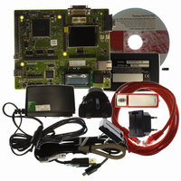
R0K572030S000BE Renesas Electronics America, R0K572030S000BE Datasheet - Page 267

R0K572030S000BE
Manufacturer Part Number
R0K572030S000BE
Description
KIT DEV FOR SH7203
Manufacturer
Renesas Electronics America
Series
Renesas Starter Kits (RSK)r
Type
MCUr
Specifications of R0K572030S000BE
Contents
CPU Board, LCD Module, E10A-Lite Emulator, Cable, QuickStart Guide and CD-ROM
Silicon Manufacturer
Renesas
Kit Contents
Board
Silicon Family Name
SH7203
Silicon Core Number
R5S72030W200FP
Tool / Board Applications
General Purpose MCU, MPU, DSP, DSC
Mcu Supported Families
SH7203
Lead Free Status / RoHS Status
Contains lead / RoHS non-compliant
For Use With/related Products
SH7203
Lead Free Status / Rohs Status
Compliant
- Current page: 267 of 1686
- Download datasheet (10Mb)
memory write-backs are performed, the value of the lower four address bits changes from H'0 to
H'4, H'8, and H'C, in that order.
(3)
ways for the entry specified by the address field are compared with the tag address that is specified
by the data field. Write the U bit (only for operand cache) and the V bit specified by the data field
to the entry of the way that has a hit. However, the tag address and LRU bits remain unchanged.
When there is no way that has a hit, nothing is written and there is no operation.
This function is used to invalidate a specific entry in the cache. When the U bit of the entry that
has had a hit is 1 in the operand cache, writing back should be performed. However, when 0 is
written to the V bit, 0 must also be written to the U bit of that entry. When memory write-backs
are performed, the value of the lower four address bits changes from H'0 to H'4, H'8, and H'C, in
that order.
8.4.2
To access a data array, the 32-bit address field (for read/write accesses) and 32-bit data field (for
write accesses) must be specified. The address field specifies information for selecting the entry to
be accessed; the data field specifies the longword data to be written to the data array.
Specify the entry address for selecting the entry, the L bit indicating the longword position within
the (16-byte) line, and the W bit for selecting the way. In the L bit, B'00 is longword 0, B'01 is
longword 1, B'10 is longword 2, and B'11 is longword 3. In the W bit, B'00 is way 0, B'01 is way
1, B'10 is way 2, and B'11 is way 3. Since the access size of the data array is fixed at longword,
specify B'00 for bits 1 and 0 of the address.
For the address and data formats, see figure 8.4.
The following two operations are possible for the data array. Information in the address array is
not modified by this operation.
(1)
The data specified by the L bit in the address is read from the entry address specified by the
address and the entry corresponding to the way.
When writing with the associative bit (A bit) of the address field set to 1, the addresses in the four
Address-Array Write (Associative Operation)
Data Array Read
Data Array
Rev. 3.00 Sep. 28, 2009 Page 235 of 1650
REJ09B0313-0300
Section 8 Cache
Related parts for R0K572030S000BE
Image
Part Number
Description
Manufacturer
Datasheet
Request
R

Part Number:
Description:
KIT STARTER FOR M16C/29
Manufacturer:
Renesas Electronics America
Datasheet:

Part Number:
Description:
KIT STARTER FOR R8C/2D
Manufacturer:
Renesas Electronics America
Datasheet:

Part Number:
Description:
R0K33062P STARTER KIT
Manufacturer:
Renesas Electronics America
Datasheet:

Part Number:
Description:
KIT STARTER FOR R8C/23 E8A
Manufacturer:
Renesas Electronics America
Datasheet:

Part Number:
Description:
KIT STARTER FOR R8C/25
Manufacturer:
Renesas Electronics America
Datasheet:

Part Number:
Description:
KIT STARTER H8S2456 SHARPE DSPLY
Manufacturer:
Renesas Electronics America
Datasheet:

Part Number:
Description:
KIT STARTER FOR R8C38C
Manufacturer:
Renesas Electronics America
Datasheet:

Part Number:
Description:
KIT STARTER FOR R8C35C
Manufacturer:
Renesas Electronics America
Datasheet:

Part Number:
Description:
KIT STARTER FOR R8CL3AC+LCD APPS
Manufacturer:
Renesas Electronics America
Datasheet:

Part Number:
Description:
KIT STARTER FOR RX610
Manufacturer:
Renesas Electronics America
Datasheet:

Part Number:
Description:
KIT STARTER FOR R32C/118
Manufacturer:
Renesas Electronics America
Datasheet:

Part Number:
Description:
KIT DEV RSK-R8C/26-29
Manufacturer:
Renesas Electronics America
Datasheet:

Part Number:
Description:
KIT STARTER FOR SH7124
Manufacturer:
Renesas Electronics America
Datasheet:

Part Number:
Description:
KIT STARTER FOR H8SX/1622
Manufacturer:
Renesas Electronics America
Datasheet:

Part Number:
Description:
KIT STARTER FOR R8C/18191A1B
Manufacturer:
Renesas Electronics America
Datasheet:


