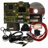
R0K572030S000BE Renesas Electronics America, R0K572030S000BE Datasheet - Page 411

R0K572030S000BE
Manufacturer Part Number
R0K572030S000BE
Description
KIT DEV FOR SH7203
Manufacturer
Renesas Electronics America
Series
Renesas Starter Kits (RSK)r
Type
MCUr
Specifications of R0K572030S000BE
Contents
CPU Board, LCD Module, E10A-Lite Emulator, Cable, QuickStart Guide and CD-ROM
Silicon Manufacturer
Renesas
Kit Contents
Board
Silicon Family Name
SH7203
Silicon Core Number
R5S72030W200FP
Tool / Board Applications
General Purpose MCU, MPU, DSP, DSC
Mcu Supported Families
SH7203
Lead Free Status / RoHS Status
Contains lead / RoHS non-compliant
For Use With/related Products
SH7203
Lead Free Status / Rohs Status
Compliant
- Current page: 411 of 1686
- Download datasheet (10Mb)
9.5.11
The burst ROM (clocked synchronous) interface is supported to access a ROM with a
synchronous burst function at high speed. The burst ROM interface accesses the burst ROM in the
same way as a normal space. This interface is valid only for area 0.
In the first access cycle, wait cycles are inserted. In this case, the number of wait cycles to be
inserted is specified by the W3 to W0 bits in CS0WCR. In the second and subsequent cycles, the
number of wait cycles to be inserted is specified by the BW1 and BW0 bits in CS0WCR.
While the burst ROM (clocked synchronous) is accessed, the BS signal is asserted only for the
first access cycle and an external wait input is also valid for the first access cycle.
If the bus width is 16 bits, the burst length must be specified as 8. If the bus width is 32 bits, the
burst length must be specified as 4. The burst ROM interface does not support the 8-bit bus width
for the burst ROM.
The burst ROM interface performs burst operations for all read access. For example, in a
longword access over a 16-bit bus, valid 16-bit data is read two times and invalid 16-bit data is
read six times. These invalid data read cycles increase the memory access time and degrade the
program execution speed and DMA transfer speed. To prevent this problem, it is recommended
using a 16-byte read by cache fill in the cache-enabled spaces or 16-byte read by the DMA. The
burst ROM interface performs write access in the same way as normal space access.
D15 to D0
A25 to A0
DACKn*
RD/WR
CKIO
WAIT
CS0
RD
BS
Note: * The waveform for DACKn is when active low is specified.
Burst ROM (Clocked Synchronous) Interface
T1
Wait Cycles Inserted in Second and Subsequent Access Cycles = 1)
Figure 9.52 Burst ROM Access Timing (Clocked Synchronous)
Tw
(Burst Length = 8, Wait Cycles Inserted in First Access = 2,
Tw
T2B
Twb
T2B
Twb
T2B
Twb
T2B
Twb
Rev. 3.00 Sep. 28, 2009 Page 379 of 1650
T2B
Section 9 Bus State Controller (BSC)
Twb
T2B
Twb
T2B
REJ09B0313-0300
Twb
T2
Related parts for R0K572030S000BE
Image
Part Number
Description
Manufacturer
Datasheet
Request
R

Part Number:
Description:
KIT STARTER FOR M16C/29
Manufacturer:
Renesas Electronics America
Datasheet:

Part Number:
Description:
KIT STARTER FOR R8C/2D
Manufacturer:
Renesas Electronics America
Datasheet:

Part Number:
Description:
R0K33062P STARTER KIT
Manufacturer:
Renesas Electronics America
Datasheet:

Part Number:
Description:
KIT STARTER FOR R8C/23 E8A
Manufacturer:
Renesas Electronics America
Datasheet:

Part Number:
Description:
KIT STARTER FOR R8C/25
Manufacturer:
Renesas Electronics America
Datasheet:

Part Number:
Description:
KIT STARTER H8S2456 SHARPE DSPLY
Manufacturer:
Renesas Electronics America
Datasheet:

Part Number:
Description:
KIT STARTER FOR R8C38C
Manufacturer:
Renesas Electronics America
Datasheet:

Part Number:
Description:
KIT STARTER FOR R8C35C
Manufacturer:
Renesas Electronics America
Datasheet:

Part Number:
Description:
KIT STARTER FOR R8CL3AC+LCD APPS
Manufacturer:
Renesas Electronics America
Datasheet:

Part Number:
Description:
KIT STARTER FOR RX610
Manufacturer:
Renesas Electronics America
Datasheet:

Part Number:
Description:
KIT STARTER FOR R32C/118
Manufacturer:
Renesas Electronics America
Datasheet:

Part Number:
Description:
KIT DEV RSK-R8C/26-29
Manufacturer:
Renesas Electronics America
Datasheet:

Part Number:
Description:
KIT STARTER FOR SH7124
Manufacturer:
Renesas Electronics America
Datasheet:

Part Number:
Description:
KIT STARTER FOR H8SX/1622
Manufacturer:
Renesas Electronics America
Datasheet:

Part Number:
Description:
KIT STARTER FOR R8C/18191A1B
Manufacturer:
Renesas Electronics America
Datasheet:


