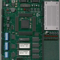
MPC555CME Freescale Semiconductor, MPC555CME Datasheet - Page 935

MPC555CME
Manufacturer Part Number
MPC555CME
Description
KIT EVALUATION FOR MPC555
Manufacturer
Freescale Semiconductor
Type
Microcontrollerr
Datasheet
1.MPC555CME.pdf
(966 pages)
Specifications of MPC555CME
Contents
Module Board, Installation Guide, Power Supply, Cable, Software and more
Processor To Be Evaluated
MPC555
Data Bus Width
32 bit
Interface Type
RS-232
For Use With/related Products
MPC555
Lead Free Status / RoHS Status
Contains lead / RoHS non-compliant
- Current page: 935 of 966
- Download datasheet (13Mb)
G.18 GPIO Electrical Characteristics
G.19 TPU3 Electrical Characteristics
MPC555 / MPC556
USER’S MANUAL
122
123
Num
Num
124
125 CLKOUT High to TPU Output Channel Hold
126 TPU Input Channel Pulse Width
NOTES:
NOTES:
1. GPIO applies to all pins used as GPIO: SGPIOA[8:31], SQPIOD[0:31], SGPIOC[0:7], QGPIO[0:6], QGPO[1:2],
2. This parameter is tested during initial characterization and is not tested in production.
3. Care should be taken to insure that the total power dissipation of the device remain below the absolute maxi-
1. AC timing is shown with respect to 10% V
2. Timing not valid for external T2CLK input.
3. Care should be taken to insure that the total power dissipation of the device remain below the absolute maxi-
4. t
MPIO[0:15], A_PQA[0:7], B_PQA[0:7], A_PQB[0:7] (inputs only), B_PQB[0:7] (inputs only).
mum rating under this condition. See
user must insure that the pin is always configured as an output and set to slow slew rate mode (SLR0 of PD-
MCR = 0). Do not change SLR0 of PDMCR to a 1 under these conditions.
larger.
mum rating under this condition. See
pin is always configured as an output.
Rise Time
Input
Output
Output
Output (SLR0 of PDMCR = 1), up to 50 pF Load
Fall Time
Input
Output
Output
Output (SLR0 of PDMCR = 1), up to 50 pF Load
Slew Rate of TPU Output Channel Valid
(SLR0 of PDMCR = 0, 50 pF to 200 pF Load)
(SLR0 of PDMCR = 0, up to 20 nF Load)
(SLR0 of PDMCR = 1, up to 50 pF Load)
cyc
is defined as the IMB Clock Period.
2
2
2
2
(SLR0 of PDMCR = 0), 50 pF to 200 pF Load
(SLR0 of PDMCR = 0), 50 pF to 200 pF Load
(SLR0 of PDMCR = 0), up to 20 nF Load
(SLR0 of PDMCR = 0), up to 20 nF Load
ELECTRICAL CHARACTERISTICS
Rating
Rating
4
Table G-18 GPIO Timing
Table G-19 TPU3 Timing
Table
Table
Rev. 15 October 2000
1,2
3
DDH
(T
(T
G-1. With a capacitive load > 20 nF (up to 100 nF maximum), the
G-1. With a capacitive load > 20 nF, the user must insure that the
A
A
= T
= T
and 90% V
3
3
L
L
to T
to T
H
H
)
)
DDH
levels. Total slew rate from 0 to V
1
Symbol
Symbol
t
t
CHTOH
CHTOV
t
TIPW
t
t
t
t
ro
fo
ri
fi
2000
2000
2000
Min
Min
90
90
92
—
—
3
0
4
3
3
7550
7500
7500
Max
Max
600
600
650
MOTOROLA
25
15
25
25
—
1
1
DDH
will be
Unit
Unit
t
G-57
µs
ns
ns
ns
µs
ns
ns
ns
ns
ns
cyc
Related parts for MPC555CME
Image
Part Number
Description
Manufacturer
Datasheet
Request
R

Part Number:
Description:
MPC555 Interrupts
Manufacturer:
Freescale Semiconductor / Motorola
Datasheet:
Part Number:
Description:
Manufacturer:
Freescale Semiconductor, Inc
Datasheet:
Part Number:
Description:
Manufacturer:
Freescale Semiconductor, Inc
Datasheet:
Part Number:
Description:
Manufacturer:
Freescale Semiconductor, Inc
Datasheet:
Part Number:
Description:
Manufacturer:
Freescale Semiconductor, Inc
Datasheet:
Part Number:
Description:
Manufacturer:
Freescale Semiconductor, Inc
Datasheet:
Part Number:
Description:
Manufacturer:
Freescale Semiconductor, Inc
Datasheet:
Part Number:
Description:
Manufacturer:
Freescale Semiconductor, Inc
Datasheet:
Part Number:
Description:
Manufacturer:
Freescale Semiconductor, Inc
Datasheet:
Part Number:
Description:
Manufacturer:
Freescale Semiconductor, Inc
Datasheet:
Part Number:
Description:
Manufacturer:
Freescale Semiconductor, Inc
Datasheet:
Part Number:
Description:
Manufacturer:
Freescale Semiconductor, Inc
Datasheet:
Part Number:
Description:
Manufacturer:
Freescale Semiconductor, Inc
Datasheet:
Part Number:
Description:
Manufacturer:
Freescale Semiconductor, Inc
Datasheet:
Part Number:
Description:
Manufacturer:
Freescale Semiconductor, Inc
Datasheet:


