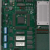
MPC555CME Freescale Semiconductor, MPC555CME Datasheet - Page 379

MPC555CME
Manufacturer Part Number
MPC555CME
Description
KIT EVALUATION FOR MPC555
Manufacturer
Freescale Semiconductor
Type
Microcontrollerr
Datasheet
1.MPC555CME.pdf
(966 pages)
Specifications of MPC555CME
Contents
Module Board, Installation Guide, Power Supply, Cable, Software and more
Processor To Be Evaluated
MPC555
Data Bus Width
32 bit
Interface Type
RS-232
For Use With/related Products
MPC555
Lead Free Status / RoHS Status
Contains lead / RoHS non-compliant
- Current page: 379 of 966
- Download datasheet (13Mb)
10.8 Programming Model
10.8.1 General Memory Controller Programming Notes
MPC555
USER’S MANUAL
The following registers are used to control the memory controller.
Note:
In all subsequent registers bit tables, if two reset values are given: the upper is for CSx, x = 1, 2, 3, and the lower
is dedicated to CS[0].
1. In the case of an external master that accesses an internal MPC555 / MPC556
2. If the memory controller serves an external master, then it can support access-
3. When the SETA bit in the base register is set, then the timing programming for
/
MPC556
module (in slave or peripheral mode), if that slave device address also matches
one of the memory controller’s regions, the memory controller will not issue any
CS for this access, nor will it terminate the cycle. Thus, this practice should be
avoided. Be aware also that any internal slave access prevents memory con-
troller operation.
es to 32-bit port devices only. This is because the MPC555 / MPC556 external
bus interface cannot initiate extra cycles to complete an access to a smaller
port-size device as it does not own the external bus.
the various strobes (CS, OE and WE/BE) may become meaningless.
0x2F C120 —
0x2F C148 —
0x2F C10C
0x2F C11C
0x2F C100
0x2F C104
0x2F C108
0x2F C110
0x2F C114
0x2F C118
0x2F C140
0x2F C144
0x2F C174
0x2F C178
Address
Table 10-5 Memory Controller Address Map
0x13F
MEMORY CONTROLLER
Rev. 15 October 2000
Dual-Mapping Option Register (DMOR)
Dual-Mapping Base Register (DMBR)
Memory Status Register (MSTAT)
Option Register Bank 0 (OR0)
Option Register Bank 1 (OR1)
Option Register Bank 2 (OR2)
Option Register Bank 3 (OR3)
Base Register Bank 0 (BR0)
Base Register Bank 1 (BR1)
Base Register Bank 2 (BR2)
Base Register Bank 3 (BR3)
Reserved
Reserved
Register
MOTOROLA
10-27
Related parts for MPC555CME
Image
Part Number
Description
Manufacturer
Datasheet
Request
R

Part Number:
Description:
MPC555 Interrupts
Manufacturer:
Freescale Semiconductor / Motorola
Datasheet:
Part Number:
Description:
Manufacturer:
Freescale Semiconductor, Inc
Datasheet:
Part Number:
Description:
Manufacturer:
Freescale Semiconductor, Inc
Datasheet:
Part Number:
Description:
Manufacturer:
Freescale Semiconductor, Inc
Datasheet:
Part Number:
Description:
Manufacturer:
Freescale Semiconductor, Inc
Datasheet:
Part Number:
Description:
Manufacturer:
Freescale Semiconductor, Inc
Datasheet:
Part Number:
Description:
Manufacturer:
Freescale Semiconductor, Inc
Datasheet:
Part Number:
Description:
Manufacturer:
Freescale Semiconductor, Inc
Datasheet:
Part Number:
Description:
Manufacturer:
Freescale Semiconductor, Inc
Datasheet:
Part Number:
Description:
Manufacturer:
Freescale Semiconductor, Inc
Datasheet:
Part Number:
Description:
Manufacturer:
Freescale Semiconductor, Inc
Datasheet:
Part Number:
Description:
Manufacturer:
Freescale Semiconductor, Inc
Datasheet:
Part Number:
Description:
Manufacturer:
Freescale Semiconductor, Inc
Datasheet:
Part Number:
Description:
Manufacturer:
Freescale Semiconductor, Inc
Datasheet:
Part Number:
Description:
Manufacturer:
Freescale Semiconductor, Inc
Datasheet:


