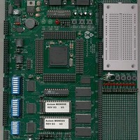
MPC555CME Freescale Semiconductor, MPC555CME Datasheet - Page 889

MPC555CME
Manufacturer Part Number
MPC555CME
Description
KIT EVALUATION FOR MPC555
Manufacturer
Freescale Semiconductor
Type
Microcontrollerr
Datasheet
1.MPC555CME.pdf
(966 pages)
Specifications of MPC555CME
Contents
Module Board, Installation Guide, Power Supply, Cable, Software and more
Processor To Be Evaluated
MPC555
Data Bus Width
32 bit
Interface Type
RS-232
For Use With/related Products
MPC555
Lead Free Status / RoHS Status
Contains lead / RoHS non-compliant
- Current page: 889 of 966
- Download datasheet (13Mb)
MPC555 / MPC556
USER’S MANUAL
6. 90 pF maximum for mask sets prior to K62N
7. All bus pins support two drive strengths capabilities, 25 pF and 50 pF. Current drive is less at the 25-pF capac-
8. Only IRQ, TPU, MIOS, GPIO, QADC (when digital inputs) and RESET pins have hysteresis, thus there is no
9. The worst case V
10. Maximum occurs during programming and erase. Read I
11. All power consumption characteristics assume 50-pF loads and running a typical application.The power con-
12. Current measured at maximum system clock frequency with QADC active.
13. This parameter is periodically sampled rather than 100% tested.
14. KAPWR and V
15. To obtain full-range results, V
16. To obtain full-range results, V
17. The voltage at which the LVSRS bits in the VSRMCR register will be set ranges from 1.5 – 2.4 V.
18. All injection current is transferred to the V
19. Total injection current for all digital input-only and all digital input/output pins must not exceed 10 mA. Exceed-
20. Below disruptive current conditions, the channel being stressed has conversion values of 0x3FF for analog
itive load. Both modes achieve 40-MHz timing.
hysteresis characteristic required for all other pins
sumption of some modules could go up is they are exercised heavier, but the power consumption of other mod-
ules would decrease.
the power supply within the specified voltage range.
ing this limit can cause disruption of normal operation.
inputs greater than V
to the presence of the sample amplifier. Other channels are not affected by non-disruptive conditions.
DDSRAM
DDF
RH
occurs during HRESET active (booting), other modules will not be running.
and $000 for values less than V
are powered up prior to any other supply.
ELECTRICAL CHARACTERISTICS
SSA
SSA
≤ V
≤ V
Rev. 15 October 2000
RL
RL
≤ V
≤ V
DDH
INDC
INDC
. An external load is required to dissipate this current to maintain
≤ V
≤ V
RH
RH
RL
≤ V
≤ V
. This assumes that V
PP
DDA
DDA
is lower.
RH
≤ V
DDA
and V
RL
MOTOROLA
≥ V
SSA
G-11
due
Related parts for MPC555CME
Image
Part Number
Description
Manufacturer
Datasheet
Request
R

Part Number:
Description:
MPC555 Interrupts
Manufacturer:
Freescale Semiconductor / Motorola
Datasheet:
Part Number:
Description:
Manufacturer:
Freescale Semiconductor, Inc
Datasheet:
Part Number:
Description:
Manufacturer:
Freescale Semiconductor, Inc
Datasheet:
Part Number:
Description:
Manufacturer:
Freescale Semiconductor, Inc
Datasheet:
Part Number:
Description:
Manufacturer:
Freescale Semiconductor, Inc
Datasheet:
Part Number:
Description:
Manufacturer:
Freescale Semiconductor, Inc
Datasheet:
Part Number:
Description:
Manufacturer:
Freescale Semiconductor, Inc
Datasheet:
Part Number:
Description:
Manufacturer:
Freescale Semiconductor, Inc
Datasheet:
Part Number:
Description:
Manufacturer:
Freescale Semiconductor, Inc
Datasheet:
Part Number:
Description:
Manufacturer:
Freescale Semiconductor, Inc
Datasheet:
Part Number:
Description:
Manufacturer:
Freescale Semiconductor, Inc
Datasheet:
Part Number:
Description:
Manufacturer:
Freescale Semiconductor, Inc
Datasheet:
Part Number:
Description:
Manufacturer:
Freescale Semiconductor, Inc
Datasheet:
Part Number:
Description:
Manufacturer:
Freescale Semiconductor, Inc
Datasheet:
Part Number:
Description:
Manufacturer:
Freescale Semiconductor, Inc
Datasheet:


