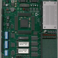
MPC555CME Freescale Semiconductor, MPC555CME Datasheet - Page 669

MPC555CME
Manufacturer Part Number
MPC555CME
Description
KIT EVALUATION FOR MPC555
Manufacturer
Freescale Semiconductor
Type
Microcontrollerr
Datasheet
1.MPC555CME.pdf
(966 pages)
Specifications of MPC555CME
Contents
Module Board, Installation Guide, Power Supply, Cable, Software and more
Processor To Be Evaluated
MPC555
Data Bus Width
32 bit
Interface Type
RS-232
For Use With/related Products
MPC555
Lead Free Status / RoHS Status
Contains lead / RoHS non-compliant
- Current page: 669 of 966
- Download datasheet (13Mb)
19.4 Array Read Operation
MPC555
USER’S MANUAL
CMFCFIG — Hard Reset Configuration Word
PRPM
EARB
MSB
16
0
During reset the HC bit (“has configuration,” bit 20) and the USIU configure the CMF
EEPROM module to provide CMFCFIG. If HC = 0 and the USIU requests internal con-
figuration during reset the reset configuration word will be provided by CMFCFIG.
The default reset state of the CMFCFIG after an erase operation of the CMF module
A block 0 is no configuration word available (HC = 1).
The CMF EEPROM array is available for read operation under most conditions while
the device is powered up. Reads of the array are not allowed under any of the following
conditions:
During programming and erase operations, while the high voltage is applied to the ar-
ray, the BIU does not acknowledge a CMF array read. At certain points, as defined in
the program or erase sequence, reading the array results in a margin read. These mar-
gin reads return the status of the program or erase operation and not the data in the
array.
The type of CMF EEPROM array read is determined by comparing the address of the
requested information with the address of the read page buffers. If the requested ad-
dress is not within one of the read page buffers or if the read page buffer has been
made invalid, an off-page read results. This read updates the read page buffer address
of the selected array block, copies the information from the array into the read page
buffer, and drives a word onto the data bus. The off-page read requires a minimum of
two clocks, while margin off-page reads require additional clocks.
If the address of the requested information is within the address ranges of either of the
read page buffers, an on-page read is performed. This requires one clock to transfer
information from the read page buffer onto the data bus. See section
PROM Array Addressing
• During master or soft reset
• ACCESS = 0 and CENSOR[0:1] = 11 or 00
• While the CMF EEPROM is disabled
17
IP
/
1
MPC556
SC
BDRV
18
2
ETRE FLEN
BDIS
19
3
20
4
BPS
COMP
EN_
21
5
for more information on array accesses.
CDR MoneT FLASH EEPROM
COMP
EXC_
Rev. 15 October 2000
22
6
RESERVED
23
7
24
8
Reserved
25
9
DBGC
10
26
DBPC ATWC
11
27
12
28
19.2.2 CMF EE-
ISB
13
29
EBDF
MOTOROLA
14
30
served
19-17
DME
LSB
Re-
15
31
Related parts for MPC555CME
Image
Part Number
Description
Manufacturer
Datasheet
Request
R

Part Number:
Description:
MPC555 Interrupts
Manufacturer:
Freescale Semiconductor / Motorola
Datasheet:
Part Number:
Description:
Manufacturer:
Freescale Semiconductor, Inc
Datasheet:
Part Number:
Description:
Manufacturer:
Freescale Semiconductor, Inc
Datasheet:
Part Number:
Description:
Manufacturer:
Freescale Semiconductor, Inc
Datasheet:
Part Number:
Description:
Manufacturer:
Freescale Semiconductor, Inc
Datasheet:
Part Number:
Description:
Manufacturer:
Freescale Semiconductor, Inc
Datasheet:
Part Number:
Description:
Manufacturer:
Freescale Semiconductor, Inc
Datasheet:
Part Number:
Description:
Manufacturer:
Freescale Semiconductor, Inc
Datasheet:
Part Number:
Description:
Manufacturer:
Freescale Semiconductor, Inc
Datasheet:
Part Number:
Description:
Manufacturer:
Freescale Semiconductor, Inc
Datasheet:
Part Number:
Description:
Manufacturer:
Freescale Semiconductor, Inc
Datasheet:
Part Number:
Description:
Manufacturer:
Freescale Semiconductor, Inc
Datasheet:
Part Number:
Description:
Manufacturer:
Freescale Semiconductor, Inc
Datasheet:
Part Number:
Description:
Manufacturer:
Freescale Semiconductor, Inc
Datasheet:
Part Number:
Description:
Manufacturer:
Freescale Semiconductor, Inc
Datasheet:


