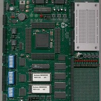
MPC555CME Freescale Semiconductor, MPC555CME Datasheet - Page 268

MPC555CME
Manufacturer Part Number
MPC555CME
Description
KIT EVALUATION FOR MPC555
Manufacturer
Freescale Semiconductor
Type
Microcontrollerr
Datasheet
1.MPC555CME.pdf
(966 pages)
Specifications of MPC555CME
Contents
Module Board, Installation Guide, Power Supply, Cable, Software and more
Processor To Be Evaluated
MPC555
Data Bus Width
32 bit
Interface Type
RS-232
For Use With/related Products
MPC555
Lead Free Status / RoHS Status
Contains lead / RoHS non-compliant
- Current page: 268 of 966
- Download datasheet (13Mb)
MPC555
USER’S MANUAL
GCLK2. When DFNH = 0, GCLK2_50 has a 50% duty cycle. With other values of
DFNH or DFNL, the duty cycle is less than 50%. Refer to
simultaneously with GCLK1. When the MPC555 / MPC556 is not in gear mode, the
falling edge of GCLK1_50 occurs in the middle of the high phase of GCLK2_50. EBDF
determines the division factor between GCLK1/GCLK2 and GCLK1_50/GCLK2_50.
During power-on reset, the MOCCK1, MODCK2, and MODCK3 pins determine the
clock source for the PLL and the clock drivers. These pins are latched on the positive
edge of PORESET. Their values must be stable as long as this line is asserted. The
configuration modes are shown in
the SPLL (OSCM or EXTCLK). MODCK1, MODCK2, and MODCK3 together deter-
mine the multiplication factor at reset and the functionality of limp mode.
If the configuration of PITRTCLK and TMBCLK and the SPLL multiplication factor is to
remain unchanged in power-down low-power mode, the MODCK signals should not
be sampled at wake-up from this mode. In this case the PORESET pin should remain
negated and HRESET should be asserted during the power supply wake-up stage.
When MODCK1 is cleared, the output of the main oscillator (OSCM) is selected as the
input to the SPLL. When MODCK1 is asserted, the external clock input (EXTCLK) is
selected as the input to the SPLL. In all cases, the system clock frequency (freq
can be reduced by the DFNH[0:2] bits in the SCCR. Note that freq
when the DFNH bits are cleared.
The TBS bit in the SCCR selects the time base clock to be either the SPLL input clock
or GCLK2. When the backup clock is functioning as the system clock, the backup clock
is automatically selected as the time base clock source.
The PITRTCLK frequency and source are specified by the RTDIV and RTSEL bits in
the SCCR. When the backup clock is functioning as the system clock, the backup
clock is automatically selected as the time base clock source.
When the PORESET pin is negated (driven to a high value), the MODCK1, MODCK2,
and MODCK3 values are not affected. They remain the same as they were defined
during the most recent power-on reset.
Table 8-1
serted).
/
MPC556
The MODCK[1:3] are shared functions with IRQ[5:7]. If IRQ[5:7] are
used as interrupts, the interrupt source should be removed during
PORESET to insure the MODCK pins are in the correct state on the
rising edge of PORESET.
shows the clock configuration modes during power-on reset (PORESET as-
CLOCKS AND POWER CONTROL
Rev. 15 October 2000
Table
NOTE
8-1. MODCK1 specifies the input source to
Figure
8-7. GCLK1_50 rises
gclk2(max)
MOTOROLA
occurs
gclk2
8-8
)
Related parts for MPC555CME
Image
Part Number
Description
Manufacturer
Datasheet
Request
R

Part Number:
Description:
MPC555 Interrupts
Manufacturer:
Freescale Semiconductor / Motorola
Datasheet:
Part Number:
Description:
Manufacturer:
Freescale Semiconductor, Inc
Datasheet:
Part Number:
Description:
Manufacturer:
Freescale Semiconductor, Inc
Datasheet:
Part Number:
Description:
Manufacturer:
Freescale Semiconductor, Inc
Datasheet:
Part Number:
Description:
Manufacturer:
Freescale Semiconductor, Inc
Datasheet:
Part Number:
Description:
Manufacturer:
Freescale Semiconductor, Inc
Datasheet:
Part Number:
Description:
Manufacturer:
Freescale Semiconductor, Inc
Datasheet:
Part Number:
Description:
Manufacturer:
Freescale Semiconductor, Inc
Datasheet:
Part Number:
Description:
Manufacturer:
Freescale Semiconductor, Inc
Datasheet:
Part Number:
Description:
Manufacturer:
Freescale Semiconductor, Inc
Datasheet:
Part Number:
Description:
Manufacturer:
Freescale Semiconductor, Inc
Datasheet:
Part Number:
Description:
Manufacturer:
Freescale Semiconductor, Inc
Datasheet:
Part Number:
Description:
Manufacturer:
Freescale Semiconductor, Inc
Datasheet:
Part Number:
Description:
Manufacturer:
Freescale Semiconductor, Inc
Datasheet:
Part Number:
Description:
Manufacturer:
Freescale Semiconductor, Inc
Datasheet:


