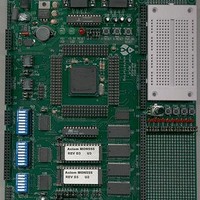
MPC555CME Freescale Semiconductor, MPC555CME Datasheet - Page 86

MPC555CME
Manufacturer Part Number
MPC555CME
Description
KIT EVALUATION FOR MPC555
Manufacturer
Freescale Semiconductor
Type
Microcontrollerr
Datasheet
1.MPC555CME.pdf
(966 pages)
Specifications of MPC555CME
Contents
Module Board, Installation Guide, Power Supply, Cable, Software and more
Processor To Be Evaluated
MPC555
Data Bus Width
32 bit
Interface Type
RS-232
For Use With/related Products
MPC555
Lead Free Status / RoHS Status
Contains lead / RoHS non-compliant
- Current page: 86 of 966
- Download datasheet (13Mb)
2.3.8.3 VDDI
2.3.8.4 VSSI
2.3.8.5 KAPWR
2.3.8.6 VDDSRAM
2.3.8.7 VSS
2.4 Reset State
2.4.1 Pin Functionality Out of Reset
MPC555
USER’S MANUAL
Pin Name: vddi
VDDI – 3-V voltage supply input for internal logic.
Pin Name: vssi
VSSI – Zero supply input for internal logic. In packaged devices, VSSI is not a sepa-
rate input from VSS.
Pin Name: kapwr
Keep-Alive Power – 3-V voltage supply input for the oscillator and keep-alive regis-
ters.
Pin Name: vddsram
SRAM Keep-Alive Power – 3-V voltage supply input for the SRAM.
Pin Name: vss
VSS – Ground level reference input.
All input pins, with the exception of the power supply and clock related pins, are “weak-
ly pulled” to a value during reset by a 130-microampere resistor based on certain con-
ditions. In reset state all I/O pins become inputs, and all outputs except clkout,
hreset_b, sreset_b, will be pulled only by the pull-up/pull-down.
The functionality out of reset of some pins that support multiple functionality is defined
in the SIUMCR through the reset configuration word. For details on which multiplexed
pins are configured by the reset configuration word and how they are configured, refer
to
The 3-V related pins have selectable output buffer drive strengths which are controlled
by the COM[0] bit in the USIU’s system clock and reset control register (SCCR). The
control is as follows:
7.5.2 Hard Reset Configuration
/
MPC556
SIGNAL DESCRIPTIONS
Rev. 15 October 2000
Word.
MOTOROLA
2-28
Related parts for MPC555CME
Image
Part Number
Description
Manufacturer
Datasheet
Request
R

Part Number:
Description:
MPC555 Interrupts
Manufacturer:
Freescale Semiconductor / Motorola
Datasheet:
Part Number:
Description:
Manufacturer:
Freescale Semiconductor, Inc
Datasheet:
Part Number:
Description:
Manufacturer:
Freescale Semiconductor, Inc
Datasheet:
Part Number:
Description:
Manufacturer:
Freescale Semiconductor, Inc
Datasheet:
Part Number:
Description:
Manufacturer:
Freescale Semiconductor, Inc
Datasheet:
Part Number:
Description:
Manufacturer:
Freescale Semiconductor, Inc
Datasheet:
Part Number:
Description:
Manufacturer:
Freescale Semiconductor, Inc
Datasheet:
Part Number:
Description:
Manufacturer:
Freescale Semiconductor, Inc
Datasheet:
Part Number:
Description:
Manufacturer:
Freescale Semiconductor, Inc
Datasheet:
Part Number:
Description:
Manufacturer:
Freescale Semiconductor, Inc
Datasheet:
Part Number:
Description:
Manufacturer:
Freescale Semiconductor, Inc
Datasheet:
Part Number:
Description:
Manufacturer:
Freescale Semiconductor, Inc
Datasheet:
Part Number:
Description:
Manufacturer:
Freescale Semiconductor, Inc
Datasheet:
Part Number:
Description:
Manufacturer:
Freescale Semiconductor, Inc
Datasheet:
Part Number:
Description:
Manufacturer:
Freescale Semiconductor, Inc
Datasheet:


