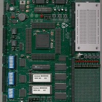
MPC555CME Freescale Semiconductor, MPC555CME Datasheet - Page 373

MPC555CME
Manufacturer Part Number
MPC555CME
Description
KIT EVALUATION FOR MPC555
Manufacturer
Freescale Semiconductor
Type
Microcontrollerr
Datasheet
1.MPC555CME.pdf
(966 pages)
Specifications of MPC555CME
Contents
Module Board, Installation Guide, Power Supply, Cable, Software and more
Processor To Be Evaluated
MPC555
Data Bus Width
32 bit
Interface Type
RS-232
For Use With/related Products
MPC555
Lead Free Status / RoHS Status
Contains lead / RoHS non-compliant
- Current page: 373 of 966
- Download datasheet (13Mb)
10.5 Write and Byte Enable Signals
10.6 Dual Mapping of the Internal Flash EEPROM Array
MPC555
USER’S MANUAL
Transfer
Word
Word
Half-
Size
Byte
The GPCM determines the timing and value of the WE/BE signals if allowed by the
port size of the accessed bank, the transfer size of the transaction and the address
accessed.
The functionality of the WE/BE[0:3] pins depends upon the value of the write enable/
byte select (WEBS) bit in the corresponding BR register. Setting WEBS to 1 will enable
these pins as BE, while resetting it to zero will enable them as WE. WE is asserted
only during write access, while BE is asserted for both read and write accesses. The
timing of the WE/BE pins remains the same in either case, and is determined by the
TRLX, ACS and CSNT bits.
The upper WE/BE (WE[0]/BE[0]) indicates that the upper eight bits of the data bus
(D0–D7) contains valid data during a write/read cycle. The upper-middle write byte en-
able (WE[1]/BE[1]) indicates that the upper-middle eight bits of the data bus (D8–D15)
contains valid data during a write/read cycle. The lower-middle write byte enable
(WE[2]/BE[2]) indicates that the lower-middle eight bits of the data bus (D16–D23)
contains valid data during a write/read cycle. The lower write/read enable (WE[3]/
BE[3]) indicates that the lower eight bits of the data bus contains valid data during a
write cycle.
The write/byte enable lines affected in a transaction for 32-bit port (PS = 00), a
16-bit port (PS = 10) and a 8-bit port (PS = 01) are shown in
shows which write enables are asserted (indicated with an ‘X’) for different combina-
tions of port size and transfer size
The user can enable mapping of the internal flash EEPROM (CMF) module to an ex-
ternal memory region controlled by the memory controller. Only one region can be pro-
grammed to be dual-mapped. When dual mapping is enabled (DME bit is set in
DMBR), an internal address matches the dual-mapped address range (as pro-
grammed in the DMBR), and the cycle type matches AT/ATM field in DMBR/DMOR
registers, then the following occur:
• The internal flash memory does not respond to that address
/
MPC556
TSIZ
0 1
0 1
0 1
0 1
1 0
1 0
0 0
A30 A31
Address
Table 10-4 Write Enable/Byte Enable Signals Function
0
0
1
1
0
1
0
0
1
0
1
0
0
0
WE[0]
BE[0]
X
X
X
/
32-bit Port Size
WE[1]
BE[1]
X
X
X
/
MEMORY CONTROLLER
Rev. 15 October 2000
WE[2]
BE[2]
X
X
X
/
WE[3]
BE[3]
X
X
X
/
WE[0]
BE[0]
X
X
X
X
X
/
16-bit Port Size
WE[1]
BE[1]
X
X
X
X
X
/
WE[2]
BE[2]
/
WE[3]
BE[3]
/
Table
WE[0]
BE[0]
X
X
X
X
X
X
X
/
8-bit Port Size
10-4. This table
WE[1]
BE[1]
/
MOTOROLA
WE[2]
BE[2]
/
10-21
WE[3]
BE[3]
/
Related parts for MPC555CME
Image
Part Number
Description
Manufacturer
Datasheet
Request
R

Part Number:
Description:
MPC555 Interrupts
Manufacturer:
Freescale Semiconductor / Motorola
Datasheet:
Part Number:
Description:
Manufacturer:
Freescale Semiconductor, Inc
Datasheet:
Part Number:
Description:
Manufacturer:
Freescale Semiconductor, Inc
Datasheet:
Part Number:
Description:
Manufacturer:
Freescale Semiconductor, Inc
Datasheet:
Part Number:
Description:
Manufacturer:
Freescale Semiconductor, Inc
Datasheet:
Part Number:
Description:
Manufacturer:
Freescale Semiconductor, Inc
Datasheet:
Part Number:
Description:
Manufacturer:
Freescale Semiconductor, Inc
Datasheet:
Part Number:
Description:
Manufacturer:
Freescale Semiconductor, Inc
Datasheet:
Part Number:
Description:
Manufacturer:
Freescale Semiconductor, Inc
Datasheet:
Part Number:
Description:
Manufacturer:
Freescale Semiconductor, Inc
Datasheet:
Part Number:
Description:
Manufacturer:
Freescale Semiconductor, Inc
Datasheet:
Part Number:
Description:
Manufacturer:
Freescale Semiconductor, Inc
Datasheet:
Part Number:
Description:
Manufacturer:
Freescale Semiconductor, Inc
Datasheet:
Part Number:
Description:
Manufacturer:
Freescale Semiconductor, Inc
Datasheet:
Part Number:
Description:
Manufacturer:
Freescale Semiconductor, Inc
Datasheet:


