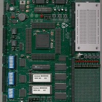
MPC555CME Freescale Semiconductor, MPC555CME Datasheet - Page 866

MPC555CME
Manufacturer Part Number
MPC555CME
Description
KIT EVALUATION FOR MPC555
Manufacturer
Freescale Semiconductor
Type
Microcontrollerr
Datasheet
1.MPC555CME.pdf
(966 pages)
Specifications of MPC555CME
Contents
Module Board, Installation Guide, Power Supply, Cable, Software and more
Processor To Be Evaluated
MPC555
Data Bus Width
32 bit
Interface Type
RS-232
For Use With/related Products
MPC555
Lead Free Status / RoHS Status
Contains lead / RoHS non-compliant
- Current page: 866 of 966
- Download datasheet (13Mb)
D.19.3.1 XFER_SIZE Greater Than 16
D.19.3.2 Data Positioning
D.19.3.3 Data Timing
MPC555 / MPC556
USER’S MANUAL
S1 SIOP_INIT
HSQ = X0
X1
S2 DATA_OUT
HSQ = X0
X1
S3 DATA_IN
HSQ = 0X
1X
NOTES:
1. Execution times do not include the time slot transition time (TST = 10 or 14 CPU clocks).
XFER_SIZE is normally programmed to be in the range 1-to-16 to match the size of
SIOP_DATA, and has thus been shown as a 5-bit value in the host interface diagram.
However, the TPU actually uses all 16 bits of the XFER_SIZE parameter when loading
BIT_COUNT. In some unusual circumstances this can be used. If an input device is
producing a data stream of greater than 16 bits then manipulation of XFER_SIZE will
allow selective capturing of the data. In clock-only mode, the extended XFER_SIZE
can be used to generate up to 0xFFFF clocks.
As stated above, no ‘justifying’ of the data position in SIOP_DATA is performed by the
TPU. This means that in the case of a byte transfer, the data output will be sourced
from one byte and the data input will shift into the other byte. This rule holds for all
data size options except 16 bits when the full SIOP_DATA register is used for both
data output and input.
In the example given in
completely synchronous with the relevant clock edge and it is assumed that the data
input is latched exactly on the opposite clock edge. This is the simplest way to show
the examples, but is not strictly true. Since the TPU is a multi-tasking system, and the
data channels are manipulated directly by microcode software while servicing the
clock edge, there is a finite delay between the relevant clock edge and the data-out
being valid or the data-in being latched. This delay is equivalent to the latency in ser-
vicing the clock channel due to other TPU activity and is shown as ‘Td’ in the timing
diagram. Td is the delay between the clock edge and the next output data being valid
and also the delay between the opposite clock edge and the input data being read. For
the vast majority of applications, the delay Td will not present a problem and can be
ignored. Only for a system which heavily loads the TPU should calculations be made
for the worst case latency for the SIOP clock channel + actual SIOP service time ( =
Td) and ensure that the baud rate is chosen such that HALF_PERIOD - Td is not less
State Number and Name
Figure
Table D-5 SIOP State Timing
TPU ROM FUNCTIONS
Rev. 15 October 2000
Max. CPU Clock Cycles
D-31, the data output transitions are shown as being
28
38
14
24
14
28
1
Number of RAM Accesses by TPU
7
7
4
4
4
6
MOTOROLA
D-52
Related parts for MPC555CME
Image
Part Number
Description
Manufacturer
Datasheet
Request
R

Part Number:
Description:
MPC555 Interrupts
Manufacturer:
Freescale Semiconductor / Motorola
Datasheet:
Part Number:
Description:
Manufacturer:
Freescale Semiconductor, Inc
Datasheet:
Part Number:
Description:
Manufacturer:
Freescale Semiconductor, Inc
Datasheet:
Part Number:
Description:
Manufacturer:
Freescale Semiconductor, Inc
Datasheet:
Part Number:
Description:
Manufacturer:
Freescale Semiconductor, Inc
Datasheet:
Part Number:
Description:
Manufacturer:
Freescale Semiconductor, Inc
Datasheet:
Part Number:
Description:
Manufacturer:
Freescale Semiconductor, Inc
Datasheet:
Part Number:
Description:
Manufacturer:
Freescale Semiconductor, Inc
Datasheet:
Part Number:
Description:
Manufacturer:
Freescale Semiconductor, Inc
Datasheet:
Part Number:
Description:
Manufacturer:
Freescale Semiconductor, Inc
Datasheet:
Part Number:
Description:
Manufacturer:
Freescale Semiconductor, Inc
Datasheet:
Part Number:
Description:
Manufacturer:
Freescale Semiconductor, Inc
Datasheet:
Part Number:
Description:
Manufacturer:
Freescale Semiconductor, Inc
Datasheet:
Part Number:
Description:
Manufacturer:
Freescale Semiconductor, Inc
Datasheet:
Part Number:
Description:
Manufacturer:
Freescale Semiconductor, Inc
Datasheet:


