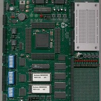
MPC555CME Freescale Semiconductor, MPC555CME Datasheet - Page 673

MPC555CME
Manufacturer Part Number
MPC555CME
Description
KIT EVALUATION FOR MPC555
Manufacturer
Freescale Semiconductor
Type
Microcontrollerr
Datasheet
1.MPC555CME.pdf
(966 pages)
Specifications of MPC555CME
Contents
Module Board, Installation Guide, Power Supply, Cable, Software and more
Processor To Be Evaluated
MPC555
Data Bus Width
32 bit
Interface Type
RS-232
For Use With/related Products
MPC555
Lead Free Status / RoHS Status
Contains lead / RoHS non-compliant
- Current page: 673 of 966
- Download datasheet (13Mb)
MPC555
USER’S MANUAL
State
S1
S2
S3
S4
Normal Operation:
Normal array reads and register accesses. The
block protect information and pulse width timing
control can be modified.
First Program Hardware Interlock Write:
Normal read operation still occurs. The array will
accept programming writes. Accesses to the regis-
ters are normal register accesses. A write to CM-
FCTL can not change EHV at this time. If the write
is to a register, no data is stored in the program
page buffers, and the CMF remains in state S2.
Expanded Program Hardware Interlock Operation:
Program margin reads will occur. Programming
writes are accepted so that all program pages may
be programmed. These writes may be to any CMF
array location. The program page buffers will be
updated using only the data, the lower address
(ADDR[26:29]) and the block address. Accesses to
the registers are normal register accesses. A write
to CMFCTL can change EHV. If the write is to a
register, no data is stored in the program page buff-
er.
Program Operation:
High voltage is applied to the array or shadow in-
formation to program the CMF bit cells. The pulse
width timer is active if SCLKR[0:2] ≠ 0 and HVS
can be polled to time the program pulse. No further
programming writes are accepted. During pro-
gramming the array does not respond to any ac-
cess. Accesses to the registers are allowed. A
write to CMFCTL can change EHV only.
/
MPC556
Table 19-9 Program Interlock State Descriptions
Mode
CDR MoneT FLASH EEPROM
Rev. 15 October 2000
State
Next
S2
S1
S3
S1
S4
S1
S5
T2
T1
T3
T6
T4
T7
T5
Write PE = 0, SES = 1
Write SES = 0 or a master reset
Hardware Interlock
A successful write to any CMF array lo-
cation. This programming write latches
the selected word of data into the pro-
gramming page buffer and the address
is latched to select the location to be
programmed. Once a bit has been writ-
ten then it will remain in the program
buffer until another write to the word or
a write of SES = 0 or a program margin
read determines that the state of the bit
needs no further modification by the
program operation. If the write is to a
register no data will be stored in the
program page buffers and the CMF will
remain in state S2.
Write SES = 0 or a master reset
Write EHV = 1
Master reset
Write EHV = 0, disable the internal
memory map or a soft reset.
Transition Requirement
MOTOROLA
19-21
Related parts for MPC555CME
Image
Part Number
Description
Manufacturer
Datasheet
Request
R

Part Number:
Description:
MPC555 Interrupts
Manufacturer:
Freescale Semiconductor / Motorola
Datasheet:
Part Number:
Description:
Manufacturer:
Freescale Semiconductor, Inc
Datasheet:
Part Number:
Description:
Manufacturer:
Freescale Semiconductor, Inc
Datasheet:
Part Number:
Description:
Manufacturer:
Freescale Semiconductor, Inc
Datasheet:
Part Number:
Description:
Manufacturer:
Freescale Semiconductor, Inc
Datasheet:
Part Number:
Description:
Manufacturer:
Freescale Semiconductor, Inc
Datasheet:
Part Number:
Description:
Manufacturer:
Freescale Semiconductor, Inc
Datasheet:
Part Number:
Description:
Manufacturer:
Freescale Semiconductor, Inc
Datasheet:
Part Number:
Description:
Manufacturer:
Freescale Semiconductor, Inc
Datasheet:
Part Number:
Description:
Manufacturer:
Freescale Semiconductor, Inc
Datasheet:
Part Number:
Description:
Manufacturer:
Freescale Semiconductor, Inc
Datasheet:
Part Number:
Description:
Manufacturer:
Freescale Semiconductor, Inc
Datasheet:
Part Number:
Description:
Manufacturer:
Freescale Semiconductor, Inc
Datasheet:
Part Number:
Description:
Manufacturer:
Freescale Semiconductor, Inc
Datasheet:
Part Number:
Description:
Manufacturer:
Freescale Semiconductor, Inc
Datasheet:


