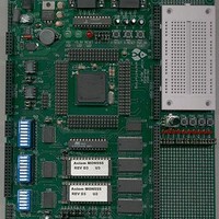
MPC555CME Freescale Semiconductor, MPC555CME Datasheet - Page 728

MPC555CME
Manufacturer Part Number
MPC555CME
Description
KIT EVALUATION FOR MPC555
Manufacturer
Freescale Semiconductor
Type
Microcontrollerr
Datasheet
1.MPC555CME.pdf
(966 pages)
Specifications of MPC555CME
Contents
Module Board, Installation Guide, Power Supply, Cable, Software and more
Processor To Be Evaluated
MPC555
Data Bus Width
32 bit
Interface Type
RS-232
For Use With/related Products
MPC555
Lead Free Status / RoHS Status
Contains lead / RoHS non-compliant
- Current page: 728 of 966
- Download datasheet (13Mb)
21.5.4 Development Serial Data Out
21.5.5 Freeze Signal
21.5.5.1 SGPIO6/FRZ/PTR Pin
21.5.5.2 IWP[0:1]/VFLS[0:1] Pins
21.5.5.3 VFLS[0:1]_MPIO32B[3:4] Pins
21.5.6 Development Port Registers
MPC555
USER’S MANUAL
The DSDI pin is also used at reset to control the overall chip configuration mode and
to determine the development port clock mode. See section
Port Serial Communications — Clock Mode Selection
The debug mode logic shifts data out of the development port shift register using the
development serial data out (DSDO) pin. All transitions on DSDO are synchronous
with DSCK or CLKOUT depending on the clock mode. Data will be valid a setup time
before the rising edge of the clock and will remain valid a hold time after the rising edge
of the clock.
Refer to
The freeze indication means that the processor is in debug mode (i.e., normal proces-
sor execution of user code is frozen). On the MPC555 / MPC556, the freeze state can
be indicated by three different pins. The FRZ signal is generated synchronously with
the system clock. This indication may be used to halt any off-chip device while in de-
bug mode as well as a handshake means between the debug tool and the debug port.
The internal freeze status can also be monitored through status in the data shifted out
of the debug port.
The SGPIO6/FRZ/PTR pin powers up as the PTR function and its function is controlled
by the GPC bits in the SIUMCR.
The IWP[0:1]/VFLS[0:1] pins power up as the VFLS[0:1] function and their function
can be changed via the DBGC bits in the SIUMCR (see
uration
Hard Reset Configuration
VFLS[0:1] pins.
The VFLS[0:1]_MPIO32B[3:4] Pins power up as the MPIO32B[3:4] function and their
function can be changed via the VFLS bit in the MIOS1TPCR register (see section
15.15.1.1). The FRZ state is indicated by the value b11 on the VFLS[0:1] pins.
The development port consists logically of the three registers: development port in-
struction register (DPIR), development port data register (DPDR), and trap enable
control register (TECR). These registers are physically implemented as two registers,
development port shift register and trap enable control register. The development port
shift register acts as both the DPIR and DPDR depending on the operation being per-
/
MPC556
Register). They can also be set via the reset configuration word (See
Table 21-12
for DSDO data meaning.
Word). The FRZ state is indicated by the value b11 on the
DEVELOPMENT SUPPORT
Rev. 15 October 2000
6.13.1.1 SIU Module Config-
for more information.
21.5.6.4 Development
MOTOROLA
7.5.2
21-32
Related parts for MPC555CME
Image
Part Number
Description
Manufacturer
Datasheet
Request
R

Part Number:
Description:
MPC555 Interrupts
Manufacturer:
Freescale Semiconductor / Motorola
Datasheet:
Part Number:
Description:
Manufacturer:
Freescale Semiconductor, Inc
Datasheet:
Part Number:
Description:
Manufacturer:
Freescale Semiconductor, Inc
Datasheet:
Part Number:
Description:
Manufacturer:
Freescale Semiconductor, Inc
Datasheet:
Part Number:
Description:
Manufacturer:
Freescale Semiconductor, Inc
Datasheet:
Part Number:
Description:
Manufacturer:
Freescale Semiconductor, Inc
Datasheet:
Part Number:
Description:
Manufacturer:
Freescale Semiconductor, Inc
Datasheet:
Part Number:
Description:
Manufacturer:
Freescale Semiconductor, Inc
Datasheet:
Part Number:
Description:
Manufacturer:
Freescale Semiconductor, Inc
Datasheet:
Part Number:
Description:
Manufacturer:
Freescale Semiconductor, Inc
Datasheet:
Part Number:
Description:
Manufacturer:
Freescale Semiconductor, Inc
Datasheet:
Part Number:
Description:
Manufacturer:
Freescale Semiconductor, Inc
Datasheet:
Part Number:
Description:
Manufacturer:
Freescale Semiconductor, Inc
Datasheet:
Part Number:
Description:
Manufacturer:
Freescale Semiconductor, Inc
Datasheet:
Part Number:
Description:
Manufacturer:
Freescale Semiconductor, Inc
Datasheet:


