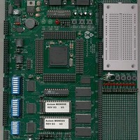
MPC555CME Freescale Semiconductor, MPC555CME Datasheet - Page 264

MPC555CME
Manufacturer Part Number
MPC555CME
Description
KIT EVALUATION FOR MPC555
Manufacturer
Freescale Semiconductor
Type
Microcontrollerr
Datasheet
1.MPC555CME.pdf
(966 pages)
Specifications of MPC555CME
Contents
Module Board, Installation Guide, Power Supply, Cable, Software and more
Processor To Be Evaluated
MPC555
Data Bus Width
32 bit
Interface Type
RS-232
For Use With/related Products
MPC555
Lead Free Status / RoHS Status
Contains lead / RoHS non-compliant
- Current page: 264 of 966
- Download datasheet (13Mb)
8.3.1 Frequency Multiplication
8.3.2 Skew Elimination
8.3.3 Pre-Divider
8.3.4 PLL Block Diagram
MPC555
USER’S MANUAL
The PLL can multiply the input frequency by any integer between one and 4096. The
multiplication factor depends on the value of the MF[0:11] bits in the PLPRCR register.
While any integer value from one to 4096 can be programmed, the resulting VCO out-
put frequency must be at least 15 MHz. The multiplication factor is set to a predeter-
mined value during power-on reset as defined in
The PLL is capable of eliminating the skew between the external clock entering the
chip (EXTCLK) and both the internal clock phases and the CLKOUT pin, making it use-
ful for tight synchronous timings. Skew elimination is active only when the PLL is en-
abled and programmed with a multiplication factor of one or two (MF = 0 or 1). The
timing reference to the system PLL is the external clock input.
A pre-divider before the phase comparator enables additional system clock resolution
when the crystal oscillator frequency is 20 MHz. The division factor is determined by
the DIVF[0:4] bits in the PLPRCR.
As shown in
tor. The phase comparator controls the direction (up or down) that the charge pump
drives the voltage across the external filter capacitor (XFC). The direction depends on
whether the feedback signal phase lags or leads the reference signal. The output of
the charge pump drives the VCO. The output frequency of the VCO is divided down
and fed back to the phase comparator for comparison with the reference signal,
OSCCLK. The MF values, zero to 4095, are mapped to multiplication factors of one to
4096. Note that when the PLL is operating in 1:1 mode (refer to
plication factor is one (MF = 0). The PLL output frequency is twice the maximum sys-
tem frequency. This double frequency is needed to generate GCLK1 and GCLK2
clocks. On power-up, with a four MHz or 20 MHz crystal and the default MF settings,
System Frequency (FREQ
The equation for system frequency (FREQ
• Skew elimination
• Frequency division
/
MPC556
System Frequency (FREQ
When operating with the backup clock, the system clock (and CLK-
OUT) is one-half of the ring oscillator frequency. (i.e., the system
clock is a nominal seven MHz). The time base and PIT clocks will be
twice the system clock frequency.
Figure
8-3, the reference signal, OSCCLK, goes to the phase compara-
CLOCKS AND POWER CONTROL
SYS
) will be 40 MHz and the system clock will be 20 MHz.
Rev. 15 October 2000
SYS
) =
NOTE
OSCCLK
DIVF + 1
SYS
) is shown below:
Table
x (MF + 1) x 2 / 2
8-1.
Table
8-1), the multi-
MOTOROLA
8-4
Related parts for MPC555CME
Image
Part Number
Description
Manufacturer
Datasheet
Request
R

Part Number:
Description:
MPC555 Interrupts
Manufacturer:
Freescale Semiconductor / Motorola
Datasheet:
Part Number:
Description:
Manufacturer:
Freescale Semiconductor, Inc
Datasheet:
Part Number:
Description:
Manufacturer:
Freescale Semiconductor, Inc
Datasheet:
Part Number:
Description:
Manufacturer:
Freescale Semiconductor, Inc
Datasheet:
Part Number:
Description:
Manufacturer:
Freescale Semiconductor, Inc
Datasheet:
Part Number:
Description:
Manufacturer:
Freescale Semiconductor, Inc
Datasheet:
Part Number:
Description:
Manufacturer:
Freescale Semiconductor, Inc
Datasheet:
Part Number:
Description:
Manufacturer:
Freescale Semiconductor, Inc
Datasheet:
Part Number:
Description:
Manufacturer:
Freescale Semiconductor, Inc
Datasheet:
Part Number:
Description:
Manufacturer:
Freescale Semiconductor, Inc
Datasheet:
Part Number:
Description:
Manufacturer:
Freescale Semiconductor, Inc
Datasheet:
Part Number:
Description:
Manufacturer:
Freescale Semiconductor, Inc
Datasheet:
Part Number:
Description:
Manufacturer:
Freescale Semiconductor, Inc
Datasheet:
Part Number:
Description:
Manufacturer:
Freescale Semiconductor, Inc
Datasheet:
Part Number:
Description:
Manufacturer:
Freescale Semiconductor, Inc
Datasheet:


