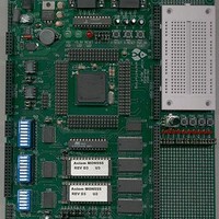
MPC555CME Freescale Semiconductor, MPC555CME Datasheet - Page 540

MPC555CME
Manufacturer Part Number
MPC555CME
Description
KIT EVALUATION FOR MPC555
Manufacturer
Freescale Semiconductor
Type
Microcontrollerr
Datasheet
1.MPC555CME.pdf
(966 pages)
Specifications of MPC555CME
Contents
Module Board, Installation Guide, Power Supply, Cable, Software and more
Processor To Be Evaluated
MPC555
Data Bus Width
32 bit
Interface Type
RS-232
For Use With/related Products
MPC555
Lead Free Status / RoHS Status
Contains lead / RoHS non-compliant
- Current page: 540 of 966
- Download datasheet (13Mb)
15.4 Block Diagram
MPC555
USER’S MANUAL
The pin prefix and suffix for the different MIOS submodules are as follows:
In the MIOS1, some pins are multiplexed between submodules using the same pin
names for the inputs and outputs which are connected as shown in
Figure 15-1
• MMCSM:
• MDASM:
• MPWMSM:
• MPIOSM:
/
— submodule short_prefix: “MC”
— pin attribute suffix: C for the Clock pin
— pin attribute suffix: L for the Load pin
— For example, an MMCSM placed as submodule number n would have its cor-
— submodule short_prefix: “DA”
— pin attribute suffix: none
— For example a MDASM placed as submodule number n would have its corre-
— submodule short_prefix: “PWM”
— pin attribute suffix: none
— For example a MPWMSM placed as submodule number n would have its cor-
— submodule short_prefix: “PIO”
— pin attribute suffix: B
— For example a MPIOSM placed as submodule number n would have its cor-
MPC556
responding input clock pin named MMCnC and its input load pin named
MMCnL. On the MPC555 / MPC556 MMC6C is input on MDA11 and MMC22C
is input on MDA13. The MMC6L is input on MDA12 and MMC22C is input on
MDA14.
sponding channel I/O pin named MDAn
responding channel I/O pin named MPWMn
responding I/O pins named MPIOnB0 to MPIOnB15 for bit-0 to bit-15, respec-
tively.
is a block diagram of the MIOS1.
MODULAR INPUT/OUTPUT SUBSYSTEM (MIOS1)
Rev. 15 October 2000
Table
15-36.
MOTOROLA
15-4
Related parts for MPC555CME
Image
Part Number
Description
Manufacturer
Datasheet
Request
R

Part Number:
Description:
MPC555 Interrupts
Manufacturer:
Freescale Semiconductor / Motorola
Datasheet:
Part Number:
Description:
Manufacturer:
Freescale Semiconductor, Inc
Datasheet:
Part Number:
Description:
Manufacturer:
Freescale Semiconductor, Inc
Datasheet:
Part Number:
Description:
Manufacturer:
Freescale Semiconductor, Inc
Datasheet:
Part Number:
Description:
Manufacturer:
Freescale Semiconductor, Inc
Datasheet:
Part Number:
Description:
Manufacturer:
Freescale Semiconductor, Inc
Datasheet:
Part Number:
Description:
Manufacturer:
Freescale Semiconductor, Inc
Datasheet:
Part Number:
Description:
Manufacturer:
Freescale Semiconductor, Inc
Datasheet:
Part Number:
Description:
Manufacturer:
Freescale Semiconductor, Inc
Datasheet:
Part Number:
Description:
Manufacturer:
Freescale Semiconductor, Inc
Datasheet:
Part Number:
Description:
Manufacturer:
Freescale Semiconductor, Inc
Datasheet:
Part Number:
Description:
Manufacturer:
Freescale Semiconductor, Inc
Datasheet:
Part Number:
Description:
Manufacturer:
Freescale Semiconductor, Inc
Datasheet:
Part Number:
Description:
Manufacturer:
Freescale Semiconductor, Inc
Datasheet:
Part Number:
Description:
Manufacturer:
Freescale Semiconductor, Inc
Datasheet:


