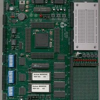
MPC555CME Freescale Semiconductor, MPC555CME Datasheet - Page 480

MPC555CME
Manufacturer Part Number
MPC555CME
Description
KIT EVALUATION FOR MPC555
Manufacturer
Freescale Semiconductor
Type
Microcontrollerr
Datasheet
1.MPC555CME.pdf
(966 pages)
Specifications of MPC555CME
Contents
Module Board, Installation Guide, Power Supply, Cable, Software and more
Processor To Be Evaluated
MPC555
Data Bus Width
32 bit
Interface Type
RS-232
For Use With/related Products
MPC555
Lead Free Status / RoHS Status
Contains lead / RoHS non-compliant
- Current page: 480 of 966
- Download datasheet (13Mb)
14.7.1.2 QSPI Control Register 1
SPCR1 — QSPI Control Register 1
14.7.1.3 QSPI Control Register 2
MPC555
USER’S MANUAL
RESET:
Bit(s)
8:15
MSB
SPE
1:7
0
0
0
SPCR1 enables the QSPI and specifies transfer delays. The CPU has read/write ac-
cess to SPCR1, but the QSPI has read access only to all bits except SPE. SPCR1
must be written last during initialization because it contains SPE. The QSPI automati-
cally clears this bit after it completes all serial transfers or when a mode fault occurs.
Writing a new value to SPCR1 while the QSPI is enabled disrupts operation.
SPCR2 contains QSPI queue pointers, wraparound mode control bits, and an interrupt
enable bit. The CPU has read/write access to SPCR2, but the QSPI has read access
only. Writes to this register are buffered. New SPCR2 values become effective only
after completion of the current serial transfer. Rewriting NEWQP in SPCR2 causes ex-
ecution to restart at the designated location. Reads of SPCR2 return the current value
of the register, not the buffer.
/
DSCKL
1
0
MPC556
Name
SPE
DTL
2
0
QSPI enable. Refer to
0 = QSPI is disabled. QSPI pins can be used for general-purpose I/O.
1 = QSPI is enabled. Pins allocated by PQSPAR are controlled by the QSPI.
Delay before SCK. When the DSCK bit is set in a command RAM byte, this field determines the
length of the delay from PCS valid to SCK transition. The following equation determines the ac-
tual delay before SCK:
where DSCKL equals is in the range of 1 to 127.
Refer to
Length of delay after transfer. When the DT bit is set in a command RAM byte, this field deter-
mines the length of the delay after a serial transfer. The following equation is used to calculate
the delay:
where DTL is in the range of 1 to 255.
A zero value for DTL causes a delay-after-transfer value of 8192 ÷ F
IMB clock).
Refer to
3
0
DSCKL
14.7.5.3 Delay Before Transfer
14.7.5.4 Delay After Transfer
QUEUED SERIAL MULTI-CHANNEL MODULE
Table 14-15 SPCR1 Bit Descriptions
4
0
5
1
14.7.4.1 Enabling, Disabling, and Halting the
Rev. 15 October 2000
6
0
7
0
Delay after Transfer
PCS to SCK Delay
for more information.
8
0
Description
for more information.
9
0
10
0
=
=
32 D
----------------------- -
DSCKL
------------------- -
f SYS
f SYS
11
0
× TL
DTL
SYS
12
0
(204.8 µs with a 40-MHz
SPI.
13
1
0x30 501A
MOTOROLA
14
0
14-18
LSB
15
0
Related parts for MPC555CME
Image
Part Number
Description
Manufacturer
Datasheet
Request
R

Part Number:
Description:
MPC555 Interrupts
Manufacturer:
Freescale Semiconductor / Motorola
Datasheet:
Part Number:
Description:
Manufacturer:
Freescale Semiconductor, Inc
Datasheet:
Part Number:
Description:
Manufacturer:
Freescale Semiconductor, Inc
Datasheet:
Part Number:
Description:
Manufacturer:
Freescale Semiconductor, Inc
Datasheet:
Part Number:
Description:
Manufacturer:
Freescale Semiconductor, Inc
Datasheet:
Part Number:
Description:
Manufacturer:
Freescale Semiconductor, Inc
Datasheet:
Part Number:
Description:
Manufacturer:
Freescale Semiconductor, Inc
Datasheet:
Part Number:
Description:
Manufacturer:
Freescale Semiconductor, Inc
Datasheet:
Part Number:
Description:
Manufacturer:
Freescale Semiconductor, Inc
Datasheet:
Part Number:
Description:
Manufacturer:
Freescale Semiconductor, Inc
Datasheet:
Part Number:
Description:
Manufacturer:
Freescale Semiconductor, Inc
Datasheet:
Part Number:
Description:
Manufacturer:
Freescale Semiconductor, Inc
Datasheet:
Part Number:
Description:
Manufacturer:
Freescale Semiconductor, Inc
Datasheet:
Part Number:
Description:
Manufacturer:
Freescale Semiconductor, Inc
Datasheet:
Part Number:
Description:
Manufacturer:
Freescale Semiconductor, Inc
Datasheet:


