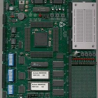
MPC555CME Freescale Semiconductor, MPC555CME Datasheet - Page 675

MPC555CME
Manufacturer Part Number
MPC555CME
Description
KIT EVALUATION FOR MPC555
Manufacturer
Freescale Semiconductor
Type
Microcontrollerr
Datasheet
1.MPC555CME.pdf
(966 pages)
Specifications of MPC555CME
Contents
Module Board, Installation Guide, Power Supply, Cable, Software and more
Processor To Be Evaluated
MPC555
Data Bus Width
32 bit
Interface Type
RS-232
For Use With/related Products
MPC555
Lead Free Status / RoHS Status
Contains lead / RoHS non-compliant
- Current page: 675 of 966
- Download datasheet (13Mb)
19.5.3 Over-Programming
19.6 Erasing CMF Array Blocks
19.6.1 Erase Sequence
MPC555
USER’S MANUAL
Either of the following events results in an over-programmed state:
Once a CMF bit has been over-programmed, data in the array block (32 Kbytes) that
is located in the same column is lost, since the over-programmed bit causes the entire
column to appear programmed. To restore an array block with an over-programmed
bit, the block must be erased.
To modify the charge stored in the isolated element of the CMF bit from a logic zero
state to a logic one state, an erase operation is required. The erase operation cannot
change the logic one state to a logic zero state; this is accomplished by the program
operation. In the CMF EEPROM, erase is a bulk operation that affects the stored
charge of all the isolated elements in an array block.
To make the CMF module block-erasable, the array is divided into blocks that are
physically isolated from each other. Each of the array blocks may be erased in isola-
tion or in any combination. The CMF array block size is fixed for all blocks in the mod-
ule at 32 Kbytes. CMF module A consists of eight array blocks; CMF module B
consists of six blocks. Array blocks of the CMF EEPROM that are protected (PRO-
TECT[M] = 1) are not erased. In addition, if EPEE = 0 no erase voltages are applied
to the array.
The array blocks selected for erase operation are determined by BLOCK[0:7] and the
array configuration.
The CMF EEPROM module requires a sequence of writes to the high voltage control
register (CMFCTL) and an erase interlock write in order to enable the high voltage to
the array and shadow information for erase operation. See
rithm bit settings.The erase sequence follows.
• Programming a CMF bit without a program margin read after each program pulse
• Exceeding the specified program times or voltages
1. Write PROTECT[0:7] to disable protect for the blocks to be erased.
2. Write PAWS to 0b100, NVR to 1, and GDB to 1.
3. Using
/
MPC556
the pulse width timing control fields for an erase pulse, BLOCK[0:7] to select the
blocks to be erased, PE = 1 and SES = 1 in the CMFCTL register. Set the initial
Failure to read each page that is being programmed after each pro-
gram pulse may result in the loss of information in the CMF EEPROM
array. While this will not physically damage the array a full erase of
all blocks being programmed must be performed before the CMF EE-
PROM can be used reliably. For more information, see
Programming.
19.7.6 A Technique to Determine SCLKR, CLKPE, and
CDR MoneT FLASH EEPROM
Rev. 15 October 2000
CAUTION
Table 19-5
19.5.3 Over-
for erase algo-
CLKPM, write
MOTOROLA
19-23
Related parts for MPC555CME
Image
Part Number
Description
Manufacturer
Datasheet
Request
R

Part Number:
Description:
MPC555 Interrupts
Manufacturer:
Freescale Semiconductor / Motorola
Datasheet:
Part Number:
Description:
Manufacturer:
Freescale Semiconductor, Inc
Datasheet:
Part Number:
Description:
Manufacturer:
Freescale Semiconductor, Inc
Datasheet:
Part Number:
Description:
Manufacturer:
Freescale Semiconductor, Inc
Datasheet:
Part Number:
Description:
Manufacturer:
Freescale Semiconductor, Inc
Datasheet:
Part Number:
Description:
Manufacturer:
Freescale Semiconductor, Inc
Datasheet:
Part Number:
Description:
Manufacturer:
Freescale Semiconductor, Inc
Datasheet:
Part Number:
Description:
Manufacturer:
Freescale Semiconductor, Inc
Datasheet:
Part Number:
Description:
Manufacturer:
Freescale Semiconductor, Inc
Datasheet:
Part Number:
Description:
Manufacturer:
Freescale Semiconductor, Inc
Datasheet:
Part Number:
Description:
Manufacturer:
Freescale Semiconductor, Inc
Datasheet:
Part Number:
Description:
Manufacturer:
Freescale Semiconductor, Inc
Datasheet:
Part Number:
Description:
Manufacturer:
Freescale Semiconductor, Inc
Datasheet:
Part Number:
Description:
Manufacturer:
Freescale Semiconductor, Inc
Datasheet:
Part Number:
Description:
Manufacturer:
Freescale Semiconductor, Inc
Datasheet:


