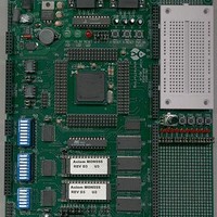
MPC555CME Freescale Semiconductor, MPC555CME Datasheet - Page 729

MPC555CME
Manufacturer Part Number
MPC555CME
Description
KIT EVALUATION FOR MPC555
Manufacturer
Freescale Semiconductor
Type
Microcontrollerr
Datasheet
1.MPC555CME.pdf
(966 pages)
Specifications of MPC555CME
Contents
Module Board, Installation Guide, Power Supply, Cable, Software and more
Processor To Be Evaluated
MPC555
Data Bus Width
32 bit
Interface Type
RS-232
For Use With/related Products
MPC555
Lead Free Status / RoHS Status
Contains lead / RoHS non-compliant
- Current page: 729 of 966
- Download datasheet (13Mb)
21.5.6.1 Development Port Shift Register
21.5.6.2 Trap Enable Control Register
21.5.6.3 Development Port Registers Decode
MPC555
USER’S MANUAL
formed. It is also used as a temporary holding register for data to be stored into the
TECR. These registers are discussed below in more detail.
The development port shift register is a 35-bit shift register. Instructions and data are
shifted into it serially from DSDI using DSCK (or CLKOUT depending on the debug
port clock mode, refer to
Clock Mode Selection
ferred in parallel to the CPU, the trap enable control register (TECR). When the pro-
cessor enters debug mode it fetches instructions from the DPIR which causes an
access to the development port shift register. These instructions are serially loaded
into the shift register from DSDI using DSCK (or CLKOUT) as the shift clock. In a sim-
ilar way, data is transferred to the CPU by moving it into the shift register which the
processor reads as the result of executing a “move from special purpose register DP-
DR” instruction. Data is also parallel-loaded into the development port shift register
from the CPU by executing a “move to special purpose register DPDR” instruction. It
is then shifted out serially to DSDO using DSCK (or CLKOUT) as the shift clock.
The trap enable control register is a 9-bit register that is loaded from the development
port shift register. The contents of the control register are used to drive the six trap en-
able signals, the two breakpoint signals, and the VSYNC signal to the CPU. The
“transfer data to trap enable control register” commands will cause the appropriate bits
to be transferred to the control register.
The trap enable control register is not accessed by the CPU, but instead supplies sig-
nals to the CPU. The trap enable bits, VSYNC bit, and the breakpoint bits of this reg-
ister are loaded from the development port shift register as the result of trap enable
mode transmissions. The trap enable bits are reflected in ICTRL and LCTRL2 special
registers. See
Control Register
The development port shift register is selected when the CPU accesses DPIR or DP-
DR. Accesses to these two special purpose registers occur in debug mode and appear
on the internal bus as an address and the assertion of an address attribute signal in-
dicating that a special purpose register is being accessed. The DPIR register is read
by the CPU to fetch all instructions when in debug mode and the DPDR register is read
and written to transfer data between the CPU and external development tools. The
DPIR and DPDR are pseudo registers. Decoding either of these registers will cause
the development port shift register to be accessed. The debug mode logic knows
whether the CPU is fetching instructions or reading or writing data. If what the CPU is
expecting and what the register receives from the serial port do not match (instruction
instead of data) the mismatch is used to signal a sequence error to the external devel-
opment tool.
/
MPC556
21.7.6 I-Bus Support Control Register
2.
)
as the shift clock. These instructions or data are then trans-
21.5.6.4 Development Port Serial Communications —
DEVELOPMENT SUPPORT
Rev. 15 October 2000
and
21.7.8 L-Bus Support
MOTOROLA
21-33
Related parts for MPC555CME
Image
Part Number
Description
Manufacturer
Datasheet
Request
R

Part Number:
Description:
MPC555 Interrupts
Manufacturer:
Freescale Semiconductor / Motorola
Datasheet:
Part Number:
Description:
Manufacturer:
Freescale Semiconductor, Inc
Datasheet:
Part Number:
Description:
Manufacturer:
Freescale Semiconductor, Inc
Datasheet:
Part Number:
Description:
Manufacturer:
Freescale Semiconductor, Inc
Datasheet:
Part Number:
Description:
Manufacturer:
Freescale Semiconductor, Inc
Datasheet:
Part Number:
Description:
Manufacturer:
Freescale Semiconductor, Inc
Datasheet:
Part Number:
Description:
Manufacturer:
Freescale Semiconductor, Inc
Datasheet:
Part Number:
Description:
Manufacturer:
Freescale Semiconductor, Inc
Datasheet:
Part Number:
Description:
Manufacturer:
Freescale Semiconductor, Inc
Datasheet:
Part Number:
Description:
Manufacturer:
Freescale Semiconductor, Inc
Datasheet:
Part Number:
Description:
Manufacturer:
Freescale Semiconductor, Inc
Datasheet:
Part Number:
Description:
Manufacturer:
Freescale Semiconductor, Inc
Datasheet:
Part Number:
Description:
Manufacturer:
Freescale Semiconductor, Inc
Datasheet:
Part Number:
Description:
Manufacturer:
Freescale Semiconductor, Inc
Datasheet:
Part Number:
Description:
Manufacturer:
Freescale Semiconductor, Inc
Datasheet:


