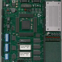
MPC555CME Freescale Semiconductor, MPC555CME Datasheet - Page 366

MPC555CME
Manufacturer Part Number
MPC555CME
Description
KIT EVALUATION FOR MPC555
Manufacturer
Freescale Semiconductor
Type
Microcontrollerr
Datasheet
1.MPC555CME.pdf
(966 pages)
Specifications of MPC555CME
Contents
Module Board, Installation Guide, Power Supply, Cable, Software and more
Processor To Be Evaluated
MPC555
Data Bus Width
32 bit
Interface Type
RS-232
For Use With/related Products
MPC555
Lead Free Status / RoHS Status
Contains lead / RoHS non-compliant
- Current page: 366 of 966
- Download datasheet (13Mb)
10.3.4 Extended Hold Time on Read Accesses
MPC555
USER’S MANUAL
In
For devices that require a long disconnection time from the data bus on read access-
es, the bit EHTR in the corresponding OR register can be set. In this case any MPC555
/ MPC556 access to the external bus following a read access to the referred memory
bank is delayed by one clock cycle unless it is a read access to the same bank.
Figure
• Because ACS = 0, TRLX being set does not delay the assertion of the CS and
• Because CSNT = 1, WE/BE is negated one clock cycle earlier than normal. (Refer
• CS is not negated one clock cycle earlier, since ACS = 00.
• The total cycle length is three clock cycles, determined as follows:
/
WE strobes.
to
— The basic memory cycle requires two clock cycles.
— One extra clock cycle is required due to the effect of TRLX on the negation of
MPC556
Address
CLOCK
Figure
RD/WR
the WE/BE strobes.
WE/BE
Data
10-12, notice the following:
OE
CS
TS
TA
10-6).
Figure 10-12 Relaxed Timing – Write Access
(ACS = 00, SCY = 0, CSNT = 1, TRLX = 1
MEMORY CONTROLLER
Rev. 15 October 2000
No Effect, ACS = 00
CSNT = 1
MOTOROLA
Figure
10-14
Related parts for MPC555CME
Image
Part Number
Description
Manufacturer
Datasheet
Request
R

Part Number:
Description:
MPC555 Interrupts
Manufacturer:
Freescale Semiconductor / Motorola
Datasheet:
Part Number:
Description:
Manufacturer:
Freescale Semiconductor, Inc
Datasheet:
Part Number:
Description:
Manufacturer:
Freescale Semiconductor, Inc
Datasheet:
Part Number:
Description:
Manufacturer:
Freescale Semiconductor, Inc
Datasheet:
Part Number:
Description:
Manufacturer:
Freescale Semiconductor, Inc
Datasheet:
Part Number:
Description:
Manufacturer:
Freescale Semiconductor, Inc
Datasheet:
Part Number:
Description:
Manufacturer:
Freescale Semiconductor, Inc
Datasheet:
Part Number:
Description:
Manufacturer:
Freescale Semiconductor, Inc
Datasheet:
Part Number:
Description:
Manufacturer:
Freescale Semiconductor, Inc
Datasheet:
Part Number:
Description:
Manufacturer:
Freescale Semiconductor, Inc
Datasheet:
Part Number:
Description:
Manufacturer:
Freescale Semiconductor, Inc
Datasheet:
Part Number:
Description:
Manufacturer:
Freescale Semiconductor, Inc
Datasheet:
Part Number:
Description:
Manufacturer:
Freescale Semiconductor, Inc
Datasheet:
Part Number:
Description:
Manufacturer:
Freescale Semiconductor, Inc
Datasheet:
Part Number:
Description:
Manufacturer:
Freescale Semiconductor, Inc
Datasheet:


