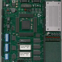
MPC555CME Freescale Semiconductor, MPC555CME Datasheet - Page 289

MPC555CME
Manufacturer Part Number
MPC555CME
Description
KIT EVALUATION FOR MPC555
Manufacturer
Freescale Semiconductor
Type
Microcontrollerr
Datasheet
1.MPC555CME.pdf
(966 pages)
Specifications of MPC555CME
Contents
Module Board, Installation Guide, Power Supply, Cable, Software and more
Processor To Be Evaluated
MPC555
Data Bus Width
32 bit
Interface Type
RS-232
For Use With/related Products
MPC555
Lead Free Status / RoHS Status
Contains lead / RoHS non-compliant
- Current page: 289 of 966
- Download datasheet (13Mb)
MPC555
USER’S MANUAL
Bit(s)
1:2
0
3
4
5
6
7
8
9
/
MPC556
DCSLR
MFPDL
STBUC
RTDIV
Name
DBCT
LPML
COM
TBS
—
Disable backup clock for timers. The DBCT bit controls the timers clock source while the chip
is in limp mode. If DBCT is set, the timers clock (tbclk, rtclk) source will not be the backup
clock, even if the system clock source is the backup clock ring oscillator. The real-time clock
source will be EXTAL or EXTCLK according to RTSEL bit (see description in bit 11 below),
and the time base clocks source will be determined according to TBS bit and MODCK1.
0 = If the chip is in limp mode, the timer clock source is the backup (limp) clock
1 = The timer clock source is either the external clock or the crystal (depending on the current
Clock output mode. These bits control the output buffer strength of the CLKOUT and external
bus pins. These bits can be dynamically changed without generating spikes on the CLKOUT
and external bus pins. If CKLOUT is not connected to external circuits, set both bits (dis-
abling CLKOUT) to minimize noise and power dissipation. COM1 is determined by the hard
reset configuration word.
00 = Clock output enabled full-strength output buffer, bus pins full drive
01 = Clock output enabled half-strength output buffer, bus pins reduced drive
10 = Clock output disabled, bus pins full drive
11 = Clock output disabled, bus pins reduced drive
Disable clock switching at loss of lock during reset. When DCSLR is clear and limp mode is
enabled, the chip will switch automaticaly to the backup clock if the PLL losses lock during
HRESET. When DCSLR is asserted, a PLL loss-of-lock event does not cause clock switch-
ing. If HRESET is asserted and DCSLR is set, the chip will not negate HRESET until the PLL
aquires lock.
0 = Enable clock switching if the PLL loses lock during reset
1 = Disable clock switching if the PLL loses lock during reset
MF and pre-divider lock. Setting this control bit disables writes to the MF and DIVF bits. This
helps prevent runaway software from changing the VCO frequency and causing the SPLL to
lose lock. In addition, to protect against hardware interference, a hardware reset will be as-
serted if these fields are changed while LPML is asserted. This bit is writable once after pow-
er-on reset.
0 = MF and DIVF fields are writable
1 = MF and DIVF fields are locked
LPM lock. Setting this control bit disables writes to the LPM and CSRC control bits. In addi-
tion, for added protection, a hardware reset is asserted if any mode is entered other than nor-
mal-high mode. This protects against runaway software causing the MCU to enter low-power
modes. (The MSR[POW] bit provides additional protection). LPML is writable once after
power-on reset.
0 = LPM and CSRC bits are writable
1 = LPM and CSRC bits are locked and hard reset will occur if the MCU is not in normal-high
Time base source. Note that when the chip is operating in limp mode (BUCS = 1), TBS is
ignored, and the backup clock is the time base clock source.
0 = Source is OSCCLK divided by either four or 16
1 = Source is system clock divided by 16
RTC (and PIT) clock divider. At power-on reset this bit is cleared if MODCK[1:3] are all low;
otherwise the bit is set.
0 = RTC and PIT clock divided by four
1 = RTC and PIT clock divided by 256
Switch to backup clock control. When software sets this bit, the system clock is switched to
the on-chip backup clock ring oscillator, and the chip undergoes a hard reset. The STBUC
bit is ignored if LME is cleared.
0 = Do not switch to the backup clock ring oscillator
1 = Switch to backup clock ring oscillator
Reserved
clock mode selected)
mode
Table 8-9 SCCR Bit Descriptions
CLOCKS AND POWER CONTROL
Rev. 15 October 2000
Description
MOTOROLA
8-29
Related parts for MPC555CME
Image
Part Number
Description
Manufacturer
Datasheet
Request
R

Part Number:
Description:
MPC555 Interrupts
Manufacturer:
Freescale Semiconductor / Motorola
Datasheet:
Part Number:
Description:
Manufacturer:
Freescale Semiconductor, Inc
Datasheet:
Part Number:
Description:
Manufacturer:
Freescale Semiconductor, Inc
Datasheet:
Part Number:
Description:
Manufacturer:
Freescale Semiconductor, Inc
Datasheet:
Part Number:
Description:
Manufacturer:
Freescale Semiconductor, Inc
Datasheet:
Part Number:
Description:
Manufacturer:
Freescale Semiconductor, Inc
Datasheet:
Part Number:
Description:
Manufacturer:
Freescale Semiconductor, Inc
Datasheet:
Part Number:
Description:
Manufacturer:
Freescale Semiconductor, Inc
Datasheet:
Part Number:
Description:
Manufacturer:
Freescale Semiconductor, Inc
Datasheet:
Part Number:
Description:
Manufacturer:
Freescale Semiconductor, Inc
Datasheet:
Part Number:
Description:
Manufacturer:
Freescale Semiconductor, Inc
Datasheet:
Part Number:
Description:
Manufacturer:
Freescale Semiconductor, Inc
Datasheet:
Part Number:
Description:
Manufacturer:
Freescale Semiconductor, Inc
Datasheet:
Part Number:
Description:
Manufacturer:
Freescale Semiconductor, Inc
Datasheet:
Part Number:
Description:
Manufacturer:
Freescale Semiconductor, Inc
Datasheet:


