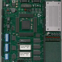
MPC555CME Freescale Semiconductor, MPC555CME Datasheet - Page 376

MPC555CME
Manufacturer Part Number
MPC555CME
Description
KIT EVALUATION FOR MPC555
Manufacturer
Freescale Semiconductor
Type
Microcontrollerr
Datasheet
1.MPC555CME.pdf
(966 pages)
Specifications of MPC555CME
Contents
Module Board, Installation Guide, Power Supply, Cable, Software and more
Processor To Be Evaluated
MPC555
Data Bus Width
32 bit
Interface Type
RS-232
For Use With/related Products
MPC555
Lead Free Status / RoHS Status
Contains lead / RoHS non-compliant
- Current page: 376 of 966
- Download datasheet (13Mb)
10.7 Memory Controller External Master Support
MPC555
USER’S MANUAL
The memory controller in the MPC555 / MPC556 supports accesses initiated by both
internal and external bus masters to external memories. If the address of any master
is mapped within the internal MPC555 / MPC556 address space, the access will be
directed to the internal device, and will be ignored by the memory controller. If the ad-
dress is not mapped internally, but rather mapped to one of the memory contoller re-
gions, the memory controller will provide the appropriate chip select and strobes as
programmed in the corresponding region (see
Register
The MPC555 / MPC556 supports only synchronous external bus masters. This means
that the external master works with CLKOUT and implements the MPC555 / MPC556
bus protocol to access a slave device.
A synchronous master initiates a transfer by asserting TS. The ADDR[0:31] signals
must be stable from the rising edge of CLKOUT during which TS is sampled, until the
last TA acknowledges the transfer. Since the external master works synchronously
with the MPC555 / MPC556, only setup and hold times around the rising edge of CLK-
OUT are important. Once the TS is detected/asserted, the memory controller com-
pares the address with each one of its defined valid banks to find a possible match.
But, since the external address space is shorter than the internal space, the actual ad-
dess that is used for comparing against the memory controller regions is in the format
of: {00000000, bits 8:16 of the external address}. In the case where a match is found,
the controls to the memory devices are generated and the transfer acknowledge indi-
cation (TA) is supplied to the master.
Since it takes two clocks for the external address to be recognized and handled by the
memory controller, the TS which is generated by the external master is ahead of the
corresponding CS and strobes which are asserted by the memory controller. This 2-
clock delay might cause problems in some synchronous memories. To overcome this,
the memory controller generates the MTS (memory transfer start) strobe which can be
used in the slave’s memory instead of the external master’s TS signal. As seen in
ure
troller so that the external memory can latch the external master’s address correctly.
To activate this feature, the MTSC bit must be set in the SIUMCR register. Refer to
6.13.1.1 SIU Module Configuration Register
When the external master accesses the internal flash when it is disabled, then the ac-
cess is terminated with transfer error acknowledge (TEA pin) asserted, and the mem-
ory controller does not support this access in any way.
When the memory controller serves an external master, the BDIP pin becomes an in-
put pin. This pin is watched by the memory controller to detect when the burst is ter-
minated.
10-18, the MTS strobe is synchronized to the assertion of CS by the memory con-
/
MPC556
(EMCR).
MEMORY CONTROLLER
Rev. 15 October 2000
for more information.
6.13.1.3 External Master Control
MOTOROLA
10-24
Fig-
Related parts for MPC555CME
Image
Part Number
Description
Manufacturer
Datasheet
Request
R

Part Number:
Description:
MPC555 Interrupts
Manufacturer:
Freescale Semiconductor / Motorola
Datasheet:
Part Number:
Description:
Manufacturer:
Freescale Semiconductor, Inc
Datasheet:
Part Number:
Description:
Manufacturer:
Freescale Semiconductor, Inc
Datasheet:
Part Number:
Description:
Manufacturer:
Freescale Semiconductor, Inc
Datasheet:
Part Number:
Description:
Manufacturer:
Freescale Semiconductor, Inc
Datasheet:
Part Number:
Description:
Manufacturer:
Freescale Semiconductor, Inc
Datasheet:
Part Number:
Description:
Manufacturer:
Freescale Semiconductor, Inc
Datasheet:
Part Number:
Description:
Manufacturer:
Freescale Semiconductor, Inc
Datasheet:
Part Number:
Description:
Manufacturer:
Freescale Semiconductor, Inc
Datasheet:
Part Number:
Description:
Manufacturer:
Freescale Semiconductor, Inc
Datasheet:
Part Number:
Description:
Manufacturer:
Freescale Semiconductor, Inc
Datasheet:
Part Number:
Description:
Manufacturer:
Freescale Semiconductor, Inc
Datasheet:
Part Number:
Description:
Manufacturer:
Freescale Semiconductor, Inc
Datasheet:
Part Number:
Description:
Manufacturer:
Freescale Semiconductor, Inc
Datasheet:
Part Number:
Description:
Manufacturer:
Freescale Semiconductor, Inc
Datasheet:


