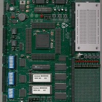
MPC555CME Freescale Semiconductor, MPC555CME Datasheet - Page 759

MPC555CME
Manufacturer Part Number
MPC555CME
Description
KIT EVALUATION FOR MPC555
Manufacturer
Freescale Semiconductor
Type
Microcontrollerr
Datasheet
1.MPC555CME.pdf
(966 pages)
Specifications of MPC555CME
Contents
Module Board, Installation Guide, Power Supply, Cable, Software and more
Processor To Be Evaluated
MPC555
Data Bus Width
32 bit
Interface Type
RS-232
For Use With/related Products
MPC555
Lead Free Status / RoHS Status
Contains lead / RoHS non-compliant
- Current page: 759 of 966
- Download datasheet (13Mb)
22.5.1 EXTEST
22.5.2 SAMPLE/PRELOAD
22.5.3 BYPASS
MPC555
USER’S MANUAL
The parallel output of the instruction register is reset to all ones in the test-logic-reset
controller state. Note that this preset state is equivalent to the BYPASS instruction.
During the capture-IR controller state, the parallel inputs to the instruction shift register
are loaded with the CLAMP command code.
The external test (EXTEST) instruction selects the 346-bit boundary scan register. EX-
TEST also asserts internal reset for the MPC555 / MPC556 system logic to force a pre-
dictable beginning internal state while performing external boundary scan operations.
By using the TAP, the register is capable of scanning user-defined values into the out-
put buffers, capturing values presented to input pins and controlling the output drive of
three-state output or bi-directional pins. For more details on the function and use of
EXTEST, refer to the scan chain document.
The SAMPLE/PRELOAD instruction initializes the boundary scan register output cells
prior to selection of EXTEST. This initialization ensures that known data will appear on
the outputs when entering the EXTEST instruction. The SAMPLE/PRELOAD instruc-
tion also provides a means to obtain a snapshot of system data and control signals.
The BYPASS instruction selects the single-bit bypass register as shown in
4. This creates a shift register path from TDI to the bypass register and, finally, to TDO,
circumventing the 463-bit boundary scan register. This instruction is used to enhance
test efficiency when a component other than the MPC555 / MPC556 becomes the de-
vice under test.
/
MPC556
Since there is no internal synchronization between the scan chain
clock (TCK) and the system clock (CLKOUT), the user must provide
some form of external synchronization to achieve meaningful results.
IEEE 1149.1-COMPLIANT INTERFACE (JTAG)
B3
0
0
0
0
0
Table 22-2 Instruction Decoding
B2
X
0
0
1
1
Code
Rev. 15 October 2000
B1
0
0
1
0
0
B0
NOTE
X
0
1
0
1
EXTEST
SAMPLE/PRELOAD
BYPASS
HI-Z
CLAMP and BYPASS
Instruction
Figure 22-
MOTOROLA
22-5
Related parts for MPC555CME
Image
Part Number
Description
Manufacturer
Datasheet
Request
R

Part Number:
Description:
MPC555 Interrupts
Manufacturer:
Freescale Semiconductor / Motorola
Datasheet:
Part Number:
Description:
Manufacturer:
Freescale Semiconductor, Inc
Datasheet:
Part Number:
Description:
Manufacturer:
Freescale Semiconductor, Inc
Datasheet:
Part Number:
Description:
Manufacturer:
Freescale Semiconductor, Inc
Datasheet:
Part Number:
Description:
Manufacturer:
Freescale Semiconductor, Inc
Datasheet:
Part Number:
Description:
Manufacturer:
Freescale Semiconductor, Inc
Datasheet:
Part Number:
Description:
Manufacturer:
Freescale Semiconductor, Inc
Datasheet:
Part Number:
Description:
Manufacturer:
Freescale Semiconductor, Inc
Datasheet:
Part Number:
Description:
Manufacturer:
Freescale Semiconductor, Inc
Datasheet:
Part Number:
Description:
Manufacturer:
Freescale Semiconductor, Inc
Datasheet:
Part Number:
Description:
Manufacturer:
Freescale Semiconductor, Inc
Datasheet:
Part Number:
Description:
Manufacturer:
Freescale Semiconductor, Inc
Datasheet:
Part Number:
Description:
Manufacturer:
Freescale Semiconductor, Inc
Datasheet:
Part Number:
Description:
Manufacturer:
Freescale Semiconductor, Inc
Datasheet:
Part Number:
Description:
Manufacturer:
Freescale Semiconductor, Inc
Datasheet:


