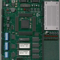
MPC555CME Freescale Semiconductor, MPC555CME Datasheet - Page 646

MPC555CME
Manufacturer Part Number
MPC555CME
Description
KIT EVALUATION FOR MPC555
Manufacturer
Freescale Semiconductor
Type
Microcontrollerr
Datasheet
1.MPC555CME.pdf
(966 pages)
Specifications of MPC555CME
Contents
Module Board, Installation Guide, Power Supply, Cable, Software and more
Processor To Be Evaluated
MPC555
Data Bus Width
32 bit
Interface Type
RS-232
For Use With/related Products
MPC555
Lead Free Status / RoHS Status
Contains lead / RoHS non-compliant
- Current page: 646 of 966
- Download datasheet (13Mb)
DPTMCR — DPT Module Configuration Register
RESET:
18.3.2 DPTRAM Test Register
RAMTST — Test Register
MPC555
USER’S MANUAL
STOP
MSB
Bit(s)
8:15
1:4
0
0
0
5
6
7
RAMTST is used only during factory testing of the MCU.
/
1
MISEN
MPC556
Name
STOP
RASP
MISF
—
—
NOT USED
2
Low power stop (sleep) mode
0 = DPTRAM clocks running
1 = DPTRAM clocks shut down
Only the STOP bit in the DPTMCR may be accessed while the STOP bit is asserted. Accesses
to other DPTRAM registers may result in unpredictable behavior. Note also that the STOP bit
should be set and cleared independently of the other control bits in this register to guarantee
proper operation. Changing the state of other bits while changing the state of the STOP bit may
result in unpredictable behavior.
Refer to
Reserved
Multiple input signature flag. MISF is readable at any time. This flag bit should be polled by the
host to determine if the MISC has completed reading the RAM. If MISF is set, the host should
read the MISRH and MISRL registers to obtain the RAM signature.
0 = First signature not ready
1 = MISC has read entire RAM. Signature is latched in MISRH and MISRL and is ready to be
Multiple input signature enable. MISEN is readable and writable at any time. The MISC will only
operate when this bit is set and the MPC555 / MPC556 is in TPU3 emulation mode. When en-
abled, the MISC will continuously cycle through the RAM addresses, reading each and adding
the contents to the MISR. In order to save power, the MISC can be disabled by clearing the MIS-
EN bit.
0 = MISC disabled
1 = MISC enabled
Ram area supervisor/user program/data. The RAM array may be placed in supervisor or unre-
stricted Space. When placed in supervisor space, (RASP = 1), only a supervisor may access the
array. If a supervisor program is accessing the array, normal read/write operation will occur. If a
user program is attempting to access the array, the access will be ignored and the address may
be decoded externally.
0 = Both supervisor and user access to RAM allowed
1 = Supervisor access only to RAM allowed
Reserved
3
read.
18.4.4 Stop Operation
Table 18-2 DPTMCR Bit Descriptions
4
MISF
DUAL-PORT TPU RAM (DPTRAM)
5
0
Rev. 15 October 2000
MIS-
EN
6
0
RASP
7
1
for more information.
8
0
Description
9
0
10
0
11
Reserved
0
12
0
13
0
0x30 0000
0x30 0002
MOTOROLA
14
0
18-4
LSB
15
0
Related parts for MPC555CME
Image
Part Number
Description
Manufacturer
Datasheet
Request
R

Part Number:
Description:
MPC555 Interrupts
Manufacturer:
Freescale Semiconductor / Motorola
Datasheet:
Part Number:
Description:
Manufacturer:
Freescale Semiconductor, Inc
Datasheet:
Part Number:
Description:
Manufacturer:
Freescale Semiconductor, Inc
Datasheet:
Part Number:
Description:
Manufacturer:
Freescale Semiconductor, Inc
Datasheet:
Part Number:
Description:
Manufacturer:
Freescale Semiconductor, Inc
Datasheet:
Part Number:
Description:
Manufacturer:
Freescale Semiconductor, Inc
Datasheet:
Part Number:
Description:
Manufacturer:
Freescale Semiconductor, Inc
Datasheet:
Part Number:
Description:
Manufacturer:
Freescale Semiconductor, Inc
Datasheet:
Part Number:
Description:
Manufacturer:
Freescale Semiconductor, Inc
Datasheet:
Part Number:
Description:
Manufacturer:
Freescale Semiconductor, Inc
Datasheet:
Part Number:
Description:
Manufacturer:
Freescale Semiconductor, Inc
Datasheet:
Part Number:
Description:
Manufacturer:
Freescale Semiconductor, Inc
Datasheet:
Part Number:
Description:
Manufacturer:
Freescale Semiconductor, Inc
Datasheet:
Part Number:
Description:
Manufacturer:
Freescale Semiconductor, Inc
Datasheet:
Part Number:
Description:
Manufacturer:
Freescale Semiconductor, Inc
Datasheet:


