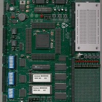
MPC555CME Freescale Semiconductor, MPC555CME Datasheet - Page 70

MPC555CME
Manufacturer Part Number
MPC555CME
Description
KIT EVALUATION FOR MPC555
Manufacturer
Freescale Semiconductor
Type
Microcontrollerr
Datasheet
1.MPC555CME.pdf
(966 pages)
Specifications of MPC555CME
Contents
Module Board, Installation Guide, Power Supply, Cable, Software and more
Processor To Be Evaluated
MPC555
Data Bus Width
32 bit
Interface Type
RS-232
For Use With/related Products
MPC555
Lead Free Status / RoHS Status
Contains lead / RoHS non-compliant
- Current page: 70 of 966
- Download datasheet (13Mb)
2.3 Signal Descriptions
2.3.1 USIU Pads
2.3.1.1 ADDR[8:31]/SGPIOA[8:31]
MPC555
USER’S MANUAL
NOTES:
VDDSRAM
VDDSYN
KAPWR
VSSSYN
1. All inputs are 5-V friendly. All 5-V outputs are slow slew rate. The QSMCM and TouCAN pins have some slew rate
2. These pins are powered by KAPWR (Keep Alive Power Supply).
3. This pin is an active negate signal and may need an external pull-up resister.
4. Drive strength was 45/90 in make sets prior to K62N.
5. Drive strength was 45/90 in make sets prior to K62N.
The pad ring supports 234 functional pins (284 including all power and ground). Each
pin and the functionality it supports are described in this section. All references to tim-
ing in this document are numbers that are expected for a typical case process with a
50-pF load at 25
V. The 5-V supply is generally referred to as the 5-V supply, and the 3.3-V supply is
referred to as the 3-V supply in this section.
Pin Name: addr_sgpioa[8:31] (24 pins)
Address Bus – Specifies the physical address of the bus transaction. The address is
driven onto the bus and kept valid until a transfer acknowledge is received from the
slave. ADDR8 is the most significant signal for this bus.
VDDH
VDDA
VDDF
EPEE
VDDL
VSSA
VSSF
VDDI
VRH
VPP
VRL
VSS
control, but are faster than the general/purpose I/O and timer pins.
Pin
/
2
MPC556
VDDSRAM
Function
VDDSYN
VSSSYN
KAPWR
VDDH
VDDA
VDDF
VDDL
VSSA
EPEE
VSSF
VDDI
VRH
VPP
VRL
VSS
Table 2-2 Pin Functionality Table (Continued)
o
C. The supply voltages are assumed to be typical, as well: 5 V or 3.3
Driver
—
—
—
—
—
—
—
—
—
—
—
—
—
—
—
—
SIGNAL DESCRIPTIONS
Rev. 15 October 2000
Type
Global Power Supplies
Sequencer
Receiver
—
—
—
—
—
—
—
—
—
—
—
—
—
—
—
CMF
Direc-
tion
I
I
I
I
I
I
I
I
I
I
I
I
I
I
I
I
1
Volt-
age
3 V
5 V
5 V
3 V
3 V
5 V
3 V
3 V
5 V
3 V
3 V
—
—
—
—
—
Slew Rate
ns / 50 pF
—
—
—
—
—
—
—
—
—
—
—
—
—
—
—
—
Strength
Drive
(pF)
MOTOROLA
—
—
—
—
—
—
—
—
—
—
—
—
—
—
—
—
Type
2-12
Pad
—
—
—
—
—
—
—
—
—
—
—
—
—
—
—
K
Related parts for MPC555CME
Image
Part Number
Description
Manufacturer
Datasheet
Request
R

Part Number:
Description:
MPC555 Interrupts
Manufacturer:
Freescale Semiconductor / Motorola
Datasheet:
Part Number:
Description:
Manufacturer:
Freescale Semiconductor, Inc
Datasheet:
Part Number:
Description:
Manufacturer:
Freescale Semiconductor, Inc
Datasheet:
Part Number:
Description:
Manufacturer:
Freescale Semiconductor, Inc
Datasheet:
Part Number:
Description:
Manufacturer:
Freescale Semiconductor, Inc
Datasheet:
Part Number:
Description:
Manufacturer:
Freescale Semiconductor, Inc
Datasheet:
Part Number:
Description:
Manufacturer:
Freescale Semiconductor, Inc
Datasheet:
Part Number:
Description:
Manufacturer:
Freescale Semiconductor, Inc
Datasheet:
Part Number:
Description:
Manufacturer:
Freescale Semiconductor, Inc
Datasheet:
Part Number:
Description:
Manufacturer:
Freescale Semiconductor, Inc
Datasheet:
Part Number:
Description:
Manufacturer:
Freescale Semiconductor, Inc
Datasheet:
Part Number:
Description:
Manufacturer:
Freescale Semiconductor, Inc
Datasheet:
Part Number:
Description:
Manufacturer:
Freescale Semiconductor, Inc
Datasheet:
Part Number:
Description:
Manufacturer:
Freescale Semiconductor, Inc
Datasheet:
Part Number:
Description:
Manufacturer:
Freescale Semiconductor, Inc
Datasheet:


