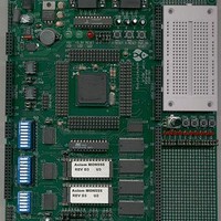
MPC555CME Freescale Semiconductor, MPC555CME Datasheet - Page 559

MPC555CME
Manufacturer Part Number
MPC555CME
Description
KIT EVALUATION FOR MPC555
Manufacturer
Freescale Semiconductor
Type
Microcontrollerr
Datasheet
1.MPC555CME.pdf
(966 pages)
Specifications of MPC555CME
Contents
Module Board, Installation Guide, Power Supply, Cable, Software and more
Processor To Be Evaluated
MPC555
Data Bus Width
32 bit
Interface Type
RS-232
For Use With/related Products
MPC555
Lead Free Status / RoHS Status
Contains lead / RoHS non-compliant
- Current page: 559 of 966
- Download datasheet (13Mb)
15.11.1.4 MDASM Status/Control Register
MDASMSCR — MDASM Status/Control Register
MPC555
USER’S MANUAL
MSB
Bit(s)
PIN
—
0
RESET:
0
1
2
3
4
5
The status/control register contains a read-only bit reflecting the status of the MDASM
pin as well as read/write bits related to its control and configuration.
* Refer to
WOR
1
0
/
FORCA
EDPOL
MPC556
Name
FREN
WOR
PIN
Table 15-16
—
FREN
2
0
Pin input status. The pin input status bit reflects the status of the corresponding pin.
Wired-OR. In the DIS, IPWM, IPM and IC modes, the WOR bit is not used; reading this bit re-
turns the value that was previously written. In the OCB, OCAB and OPWM modes, the WOR bit
selects whether the output buffer is configured for open-drain or totem-pole operation.
0 = Output buffer is totem-pole.
1 = Output buffer is open-drain.
Freeze enable. This active high read/write control bit enables the MDASM to recognize the
MIOB freeze signal.
0 = The MDASM is not frozen even if the MIOB freeze line is active.
1 = The MDASM is frozen if the MIOB freeze line is active.
0
Polarity. In the DIS mode, this bit is not used; reading it returns the last value written.
In the IPWM mode, this bit is used to select the capture edge sensitivity of channels A and B.
0 = Channel A captures on a rising edge. Channel B captures on a falling edge.
1 = Channel A captures on a falling edge. Channel B captures on a rising edge.
In the IPM and IC modes, the EDPOL bit is used to select the input capture edge sensitivity of
channel A.
0 = Channel A captures on a rising edge.
1 = Channel A captures on a falling edge.
In the OCB, OCAB and OPWM modes, the EDPOL bit is used to select the voltage level on the
output pin.
0 = The output flip-flop logic level appears on the output pin: a compare on channel A sets the
1 = The complement of the output flip-flop logic level appears on the output pin: a compare on
Force A. In the OCB, OCAB and OPWM modes, the FORCA bit allows the software to force the
output flip-flop to behave as if a successful comparison had occurred on channel A (except that
the FLAG line is not activated). Writing a one to FORCA sets the output flip-flop; writing a zero
to it has no effect.
In the DIS, IPWM, IPM and IC modes, the FORCA bit is not used and writing to it has no effect.
FORCA is cleared by reset and is always read as zero. Writing a one to both FORCA and
FORCB simultaneously resets the output flip-flop.
3
0
0
output pin, a compare on channel B resets the output pin.
channel A resets the output pin; a compare on channel B sets the output pin.
for a complete list of all the base addresses for the MDASM registers.
Table 15-17 MDASMSCR Bit Descriptions
MODULAR INPUT/OUTPUT SUBSYSTEM (MIOS1)
POL
ED-
4
0
FORC
A
5
0
FORC
Rev. 15 October 2000
B
6
0
RESERVED
7
0
8
0
Description
9
0
BSL
10
0
11
0
0
12
0
13
0
0x30 605E*
MOD
MOTOROLA
14
0
15-23
LSB
15
0
Related parts for MPC555CME
Image
Part Number
Description
Manufacturer
Datasheet
Request
R

Part Number:
Description:
MPC555 Interrupts
Manufacturer:
Freescale Semiconductor / Motorola
Datasheet:
Part Number:
Description:
Manufacturer:
Freescale Semiconductor, Inc
Datasheet:
Part Number:
Description:
Manufacturer:
Freescale Semiconductor, Inc
Datasheet:
Part Number:
Description:
Manufacturer:
Freescale Semiconductor, Inc
Datasheet:
Part Number:
Description:
Manufacturer:
Freescale Semiconductor, Inc
Datasheet:
Part Number:
Description:
Manufacturer:
Freescale Semiconductor, Inc
Datasheet:
Part Number:
Description:
Manufacturer:
Freescale Semiconductor, Inc
Datasheet:
Part Number:
Description:
Manufacturer:
Freescale Semiconductor, Inc
Datasheet:
Part Number:
Description:
Manufacturer:
Freescale Semiconductor, Inc
Datasheet:
Part Number:
Description:
Manufacturer:
Freescale Semiconductor, Inc
Datasheet:
Part Number:
Description:
Manufacturer:
Freescale Semiconductor, Inc
Datasheet:
Part Number:
Description:
Manufacturer:
Freescale Semiconductor, Inc
Datasheet:
Part Number:
Description:
Manufacturer:
Freescale Semiconductor, Inc
Datasheet:
Part Number:
Description:
Manufacturer:
Freescale Semiconductor, Inc
Datasheet:
Part Number:
Description:
Manufacturer:
Freescale Semiconductor, Inc
Datasheet:


