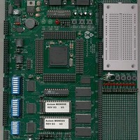
MPC555CME Freescale Semiconductor, MPC555CME Datasheet - Page 518

MPC555CME
Manufacturer Part Number
MPC555CME
Description
KIT EVALUATION FOR MPC555
Manufacturer
Freescale Semiconductor
Type
Microcontrollerr
Datasheet
1.MPC555CME.pdf
(966 pages)
Specifications of MPC555CME
Contents
Module Board, Installation Guide, Power Supply, Cable, Software and more
Processor To Be Evaluated
MPC555
Data Bus Width
32 bit
Interface Type
RS-232
For Use With/related Products
MPC555
Lead Free Status / RoHS Status
Contains lead / RoHS non-compliant
- Current page: 518 of 966
- Download datasheet (13Mb)
14.8.7.7 Receiver Functional Operation
MPC555
USER’S MANUAL
The RE bit in SCCxR1 enables (RE = 1) and disables (RE = 0) the receiver. The re-
ceiver contains a receive serial shifter and a parallel receive data register (RDRx) lo-
cated in the SCI data register (SCxDR). The serial shifter cannot be directly accessed
by the CPU. The receiver is double-buffered, allowing data to be held in the RDRx
while other data is shifted in.
Receiver bit processor logic drives a state machine that determines the logic level for
each bit-time. This state machine controls when the bit processor logic is to sample
the RXD pin and also controls when data is to be passed to the receive serial shifter.
A receive time clock is used to control sampling and synchronization. Data is shifted
into the receive serial shifter according to the most recent synchronization of the re-
ceive time clock with the incoming data stream. From this point on, data movement is
synchronized with the MCU IMB clock. Operation of the receiver state machine is de-
tailed in the
The number of bits shifted in by the receiver depends on the serial format. However,
all frames must end with at least one stop bit. When the stop bit is received, the frame
is considered to be complete, and the received data in the serial shifter is transferred
to the RDRx. The receiver data register flag (RDRF) is set when the data is trans-
ferred.
The stop bit is always a logic one. If a logic zero is sensed during this bit-time, the FE
flag in SCxSR is set. A framing error is usually caused by mismatched baud rates be-
tween the receiver and transmitter or by a significant burst of noise. Note that a framing
error is not always detected; the data in the expected stop bit-time may happen to be
a logic one.
Noise errors, parity errors, and framing errors can be detected while a data stream is
being received. Although error conditions are detected as bits are received, the noise
/
1
R
T
1
*
* Restart RT Clock
MPC556
1 1 1
R
T
1
* *
R
T
1
Queued Serial Module Reference Manual
R
T
1
* *
R
T
1
1
1
R
T
1
* *
1 1 1
R
T
1
QUEUED SERIAL MULTI-CHANNEL MODULE
Figure 14-14 Start Search Example
R
T
1
* *
R
T
1
R
T
1
0
R
T
2
Rev. 15 October 2000
0
R
T
3
R
T
4
Perceived Start Bit
0
R
T
5
Actual Start Bit
R
T
6
0 0 0 0
R
T
7
R
T
8
R
T
9
R
T
1
0 1 2 3 4 5 6
R
T
1
R
T
1
(QSMRM/AD).
R
T
1
R
T
1
R
T
1
R
T
1
*
R
T
1
R
T
2
R
T
3
LSB
MOTOROLA
14-56
Related parts for MPC555CME
Image
Part Number
Description
Manufacturer
Datasheet
Request
R

Part Number:
Description:
MPC555 Interrupts
Manufacturer:
Freescale Semiconductor / Motorola
Datasheet:
Part Number:
Description:
Manufacturer:
Freescale Semiconductor, Inc
Datasheet:
Part Number:
Description:
Manufacturer:
Freescale Semiconductor, Inc
Datasheet:
Part Number:
Description:
Manufacturer:
Freescale Semiconductor, Inc
Datasheet:
Part Number:
Description:
Manufacturer:
Freescale Semiconductor, Inc
Datasheet:
Part Number:
Description:
Manufacturer:
Freescale Semiconductor, Inc
Datasheet:
Part Number:
Description:
Manufacturer:
Freescale Semiconductor, Inc
Datasheet:
Part Number:
Description:
Manufacturer:
Freescale Semiconductor, Inc
Datasheet:
Part Number:
Description:
Manufacturer:
Freescale Semiconductor, Inc
Datasheet:
Part Number:
Description:
Manufacturer:
Freescale Semiconductor, Inc
Datasheet:
Part Number:
Description:
Manufacturer:
Freescale Semiconductor, Inc
Datasheet:
Part Number:
Description:
Manufacturer:
Freescale Semiconductor, Inc
Datasheet:
Part Number:
Description:
Manufacturer:
Freescale Semiconductor, Inc
Datasheet:
Part Number:
Description:
Manufacturer:
Freescale Semiconductor, Inc
Datasheet:
Part Number:
Description:
Manufacturer:
Freescale Semiconductor, Inc
Datasheet:


