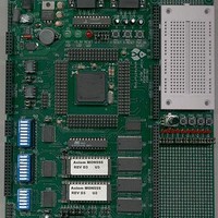
MPC555CME Freescale Semiconductor, MPC555CME Datasheet - Page 512

MPC555CME
Manufacturer Part Number
MPC555CME
Description
KIT EVALUATION FOR MPC555
Manufacturer
Freescale Semiconductor
Type
Microcontrollerr
Datasheet
1.MPC555CME.pdf
(966 pages)
Specifications of MPC555CME
Contents
Module Board, Installation Guide, Power Supply, Cable, Software and more
Processor To Be Evaluated
MPC555
Data Bus Width
32 bit
Interface Type
RS-232
For Use With/related Products
MPC555
Lead Free Status / RoHS Status
Contains lead / RoHS non-compliant
- Current page: 512 of 966
- Download datasheet (13Mb)
14.8.6 SCI Pins
14.8.7 SCI Operation
14.8.7.1 Definition of Terms
MPC555
USER’S MANUAL
Bit(s)
7:15
0:6
The RXD1 and RXD2 pins are the receive data pins for the SCI1 and SCI2, respec-
tively. TXD1 and TXD2 are the transmit data pins for the two SCI modules. An external
clock pin, ECK, is common to both SCIs. The pins and their functions are listed in
ble
The SCI can operate in polled or interrupt-driven mode. Status flags in SCxSR reflect
SCI conditions regardless of the operating mode chosen. The TIE, TCIE, RIE, and ILIE
bits in SCCxR1 enable interrupts for the conditions indicated by the TDRE, TC, RDRF,
and IDLE bits in SCxSR, respectively.
• Bit-time — The time required to transmit or receive one bit of data, which is equal
• Start bit — One bit-time of logic zero that indicates the beginning of a data frame.
• Stop bit— One bit-time of logic one that indicates the end of a data frame.
• Frame — A complete unit of serial information. The SCI can use 10-bit or 11-bit
• Data frame — A start bit, a specified number of data or information bits, and at
• Idle frame — A frame that consists of consecutive ones. An idle frame has no start
External Clock
Transmit Data
14-27.
Receive Data
/
to one cycle of the baud frequency.
A start bit must begin with a one-to-zero transition and be preceded by at least
three receive time samples of logic one.
frames.
least one stop bit.
bit.
Pin Names
R[8:0]/
MPC556
Name
T[8:0]
—
Reserved
R[7:0]/T[7:0] contain either the eight data bits received when SCxDR is read, or the eight data
bits to be transmitted when SCxDR is written. R8/T8 are used when the SCI is configured for
nine-bit operation (M = 1). When the SCI is configured for 8-bit operation, R8/T8 have no mean-
ing or effect.
Accesses to the lower byte of SCxDR triggers the mechanism for clearing the status bits or for
initiating transmissions whether byte, half-word, or word accesses are used.
QUEUED SERIAL MULTI-CHANNEL MODULE
Table 14-26 SCxSR Bit Descriptions
RXD1, RXD2
TXD1, TXD2
Mnemonic
Table 14-27 SCI Pin Functions
ECK
Rev. 15 October 2000
Receiver disabled
Receiver enabled
Transmitter disabled
Transmitter enabled
Receiver disabled
Receiver enabled
Transmitter disabled
Transmitter enabled
Mode
Description
General purpose input
Serial data input to SCI
General purpose output
Serial data output from SCI
Not used
Alternate input source to baud
Not used
Alternate input source to baud
Function
MOTOROLA
14-50
Ta-
Related parts for MPC555CME
Image
Part Number
Description
Manufacturer
Datasheet
Request
R

Part Number:
Description:
MPC555 Interrupts
Manufacturer:
Freescale Semiconductor / Motorola
Datasheet:
Part Number:
Description:
Manufacturer:
Freescale Semiconductor, Inc
Datasheet:
Part Number:
Description:
Manufacturer:
Freescale Semiconductor, Inc
Datasheet:
Part Number:
Description:
Manufacturer:
Freescale Semiconductor, Inc
Datasheet:
Part Number:
Description:
Manufacturer:
Freescale Semiconductor, Inc
Datasheet:
Part Number:
Description:
Manufacturer:
Freescale Semiconductor, Inc
Datasheet:
Part Number:
Description:
Manufacturer:
Freescale Semiconductor, Inc
Datasheet:
Part Number:
Description:
Manufacturer:
Freescale Semiconductor, Inc
Datasheet:
Part Number:
Description:
Manufacturer:
Freescale Semiconductor, Inc
Datasheet:
Part Number:
Description:
Manufacturer:
Freescale Semiconductor, Inc
Datasheet:
Part Number:
Description:
Manufacturer:
Freescale Semiconductor, Inc
Datasheet:
Part Number:
Description:
Manufacturer:
Freescale Semiconductor, Inc
Datasheet:
Part Number:
Description:
Manufacturer:
Freescale Semiconductor, Inc
Datasheet:
Part Number:
Description:
Manufacturer:
Freescale Semiconductor, Inc
Datasheet:
Part Number:
Description:
Manufacturer:
Freescale Semiconductor, Inc
Datasheet:


