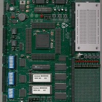
MPC555CME Freescale Semiconductor, MPC555CME Datasheet - Page 931

MPC555CME
Manufacturer Part Number
MPC555CME
Description
KIT EVALUATION FOR MPC555
Manufacturer
Freescale Semiconductor
Type
Microcontrollerr
Datasheet
1.MPC555CME.pdf
(966 pages)
Specifications of MPC555CME
Contents
Module Board, Installation Guide, Power Supply, Cable, Software and more
Processor To Be Evaluated
MPC555
Data Bus Width
32 bit
Interface Type
RS-232
For Use With/related Products
MPC555
Lead Free Status / RoHS Status
Contains lead / RoHS non-compliant
- Current page: 931 of 966
- Download datasheet (13Mb)
G.17 QSMCM Electrical Characteristics
MPC555 / MPC556
USER’S MANUAL
12. Input must be current limited to the value specified. To determine the value of the required current-limiting re-
13. This parameter is periodically sampled rather 100% tested.
14. Derate linearly to 0.3 mA if V
15. Condition applies to two adjacent pins.
16. Condition applies to all analog channels.
17. Current coupling ratio, K, is defined as the ratio of the output current, I
18. Maximum source impedance is application-dependent. Error resulting from pin leakage depends on junction
19. For a maximum sampling error of the input voltage <= 1LSB, then the external filter capacitor, C
Name
108
109
110
111
112
113
114
sistor, calculate resistance values using V
-0.3 V, then use the larger of the calculated values. The diode drop voltage is a function of current and varies
approximately 0.4 to 0.8 volts over temperature
characterization.
injection current, I
The input voltage error on the channel under test is calculated as V
leakage into the pin and on leakage due to charge-sharing with internal capacitance.
Error from junction leakage is a function of external source impedance and input leakage current. In the following
expression, expected error in result value due to junction leakage is expressed in voltage (V
V
where I
Charge-sharing leakage is a function of input source impedance, conversion rate, change in voltage between
successive conversions, and the size of the filtering capacitor used. Error levels are best determined empirically.
In general, continuous conversion of the same channel may not be compatible with high source impedance
C
errj
SAMP
= R
Operating Frequency
Master
Slave
Cycle Time
Master
Slave
Enable Lead Time
Master
Slave
Enable Lag Time
Master
Slave
Clock (SCK) High or Low Time
Master
Slave
Sequential Transfer Delay
Master
Slave (Does Not Require Deselect)
Data Setup Time (Inputs)
Master
Slave
. The value of C
OFF
S
* I
3
is a function of operating temperature.
OFF
inj
, when both adjacent pins are overstressed with the specified injection current. K = I
SAMP
(T
1
A
Function
in the new design may be reduced.
= T
DDH
L
ELECTRICAL CHARACTERISTICS
- V
to T
Table G-17 QSPI Timing
DDA
H
, 50 pF load on all QSPI pins except as noted)
Rev. 15 October 2000
= 1 volt. This characteristic is preliminary and may change after further
POSCLAMP
= (the lower of V
Symbol
t
t
qcyc
t
f
lead
t
t
t
lag
sw
op
su
td
err
DDA
= I
out
2*TC – 60
inj
, measured on the pin under test to the
2*TC – n
or V
17*TC
13*TC
4*TC
4*TC
2*TC
2*TC
2*TC
* K * R
Min
DC
DC
30
20
—
DDH
) + 0.3 V and V
S
8192*TC
510*TC
128*TC
255*TC
F
F
SCK/2
Max
SYS
SYS
—
—
—
—
—
—
—
errj
/4
/4
2
):
NEGCLAMP
MOTOROLA
f
Unit
>= 1024 *
Hz
ns
ns
ns
ns
ns
ns
out
G-53
/ I
=
inj
Related parts for MPC555CME
Image
Part Number
Description
Manufacturer
Datasheet
Request
R

Part Number:
Description:
MPC555 Interrupts
Manufacturer:
Freescale Semiconductor / Motorola
Datasheet:
Part Number:
Description:
Manufacturer:
Freescale Semiconductor, Inc
Datasheet:
Part Number:
Description:
Manufacturer:
Freescale Semiconductor, Inc
Datasheet:
Part Number:
Description:
Manufacturer:
Freescale Semiconductor, Inc
Datasheet:
Part Number:
Description:
Manufacturer:
Freescale Semiconductor, Inc
Datasheet:
Part Number:
Description:
Manufacturer:
Freescale Semiconductor, Inc
Datasheet:
Part Number:
Description:
Manufacturer:
Freescale Semiconductor, Inc
Datasheet:
Part Number:
Description:
Manufacturer:
Freescale Semiconductor, Inc
Datasheet:
Part Number:
Description:
Manufacturer:
Freescale Semiconductor, Inc
Datasheet:
Part Number:
Description:
Manufacturer:
Freescale Semiconductor, Inc
Datasheet:
Part Number:
Description:
Manufacturer:
Freescale Semiconductor, Inc
Datasheet:
Part Number:
Description:
Manufacturer:
Freescale Semiconductor, Inc
Datasheet:
Part Number:
Description:
Manufacturer:
Freescale Semiconductor, Inc
Datasheet:
Part Number:
Description:
Manufacturer:
Freescale Semiconductor, Inc
Datasheet:
Part Number:
Description:
Manufacturer:
Freescale Semiconductor, Inc
Datasheet:


