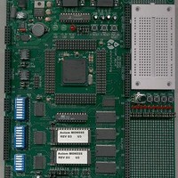
MPC555CME Freescale Semiconductor, MPC555CME Datasheet - Page 298

MPC555CME
Manufacturer Part Number
MPC555CME
Description
KIT EVALUATION FOR MPC555
Manufacturer
Freescale Semiconductor
Type
Microcontrollerr
Datasheet
1.MPC555CME.pdf
(966 pages)
Specifications of MPC555CME
Contents
Module Board, Installation Guide, Power Supply, Cable, Software and more
Processor To Be Evaluated
MPC555
Data Bus Width
32 bit
Interface Type
RS-232
For Use With/related Products
MPC555
Lead Free Status / RoHS Status
Contains lead / RoHS non-compliant
- Current page: 298 of 966
- Download datasheet (13Mb)
9.3 Bus Control Signals
MPC555
USER’S MANUAL
The MPC555 / MPC556 bus is synchronous. The bus and control input signals must
be timed to setup and hold times relative to the rising edge of the clock. Bus cycles can
be completed in two clock cycles.
For all inputs, the MPC555 / MPC556 latches the level of the input during a sample
window around the rising edge of the clock signal. This window is illustrated in
9-1, where tsu and tho are the input setup and hold times, respectively. To ensure that
an input signal is recognized on a specific falling edge of the clock, that input must be
stable during the sample window. If an input makes a transition during the window time
period, the level recognized by the MPC555 / MPC556 is not predictable; however, the
MPC555 / MPC556 always resolves the latched level to either a logic high or low be-
fore using it. In addition to meeting input setup and hold times for deterministic opera-
tion, all input signals must obey the protocols described in this section.
The MPC555 / MPC556 initiates a bus cycle by driving the address, size, address
type, cycle type, and read/write outputs. At the beginning of a bus cycle, TSIZ0 and
TSIZ1 are driven with the address type signals. TSIZ0 and TSIZ1 indicate the number
of bytes remaining to be transferred during an operand cycle (consisting of one or
more bus cycles). These signals are valid at the rising edge of the clock in which the
transfer start (TS) signal is asserted.
The read/write (RD/WR) signal determines the direction of the transfer during a bus
cycle. Driven at the beginning of a bus cycle, RD/WR is valid at the rising edge of the
clock in which TS is asserted. The logic level of RD/WR only changes when a write
cycle is preceded by a read cycle or vice versa. The signal may remain low for con-
secutive write cycles.
/
MPC556
Signal
Clock
Figure 9-1 Input Sample Window
tsu
EXTERNAL BUS INTERFACE
tho
Rev. 15 October 2000
Window
Sample
MOTOROLA
Figure
9-2
Related parts for MPC555CME
Image
Part Number
Description
Manufacturer
Datasheet
Request
R

Part Number:
Description:
MPC555 Interrupts
Manufacturer:
Freescale Semiconductor / Motorola
Datasheet:
Part Number:
Description:
Manufacturer:
Freescale Semiconductor, Inc
Datasheet:
Part Number:
Description:
Manufacturer:
Freescale Semiconductor, Inc
Datasheet:
Part Number:
Description:
Manufacturer:
Freescale Semiconductor, Inc
Datasheet:
Part Number:
Description:
Manufacturer:
Freescale Semiconductor, Inc
Datasheet:
Part Number:
Description:
Manufacturer:
Freescale Semiconductor, Inc
Datasheet:
Part Number:
Description:
Manufacturer:
Freescale Semiconductor, Inc
Datasheet:
Part Number:
Description:
Manufacturer:
Freescale Semiconductor, Inc
Datasheet:
Part Number:
Description:
Manufacturer:
Freescale Semiconductor, Inc
Datasheet:
Part Number:
Description:
Manufacturer:
Freescale Semiconductor, Inc
Datasheet:
Part Number:
Description:
Manufacturer:
Freescale Semiconductor, Inc
Datasheet:
Part Number:
Description:
Manufacturer:
Freescale Semiconductor, Inc
Datasheet:
Part Number:
Description:
Manufacturer:
Freescale Semiconductor, Inc
Datasheet:
Part Number:
Description:
Manufacturer:
Freescale Semiconductor, Inc
Datasheet:
Part Number:
Description:
Manufacturer:
Freescale Semiconductor, Inc
Datasheet:


