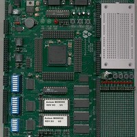
MPC555CME Freescale Semiconductor, MPC555CME Datasheet - Page 892

MPC555CME
Manufacturer Part Number
MPC555CME
Description
KIT EVALUATION FOR MPC555
Manufacturer
Freescale Semiconductor
Type
Microcontrollerr
Datasheet
1.MPC555CME.pdf
(966 pages)
Specifications of MPC555CME
Contents
Module Board, Installation Guide, Power Supply, Cable, Software and more
Processor To Be Evaluated
MPC555
Data Bus Width
32 bit
Interface Type
RS-232
For Use With/related Products
MPC555
Lead Free Status / RoHS Status
Contains lead / RoHS non-compliant
- Current page: 892 of 966
- Download datasheet (13Mb)
G.10.1 Flash Module Life
MPC555 / MPC556
USER’S MANUAL
NOTES:
NOTES:
Symbol
1. Average current is less than 30 mA when programming both modules simultaneously.
1. Target failure rate at specified number of program/erase cycles of 2 ppm pending characterization of production
2. A program/erase cycle is defined as switching the bits from 1 ➝ 0 ➝ 1.
3. Reprogramming of a CMF array block prior to erase is not required.
4. Number of program/erase cycles to be adjusted pending characterization of production silicon.
I
V
I
DDPP
V
DDF
DDF
silicon.
PP
P/E Cycles
P/E Cycles
Retention
Symbol
Operating Voltage
Read, Program or Erase
Operating Current at 40.0 MHz,
V
Read, Program or Erase Operation
Disabled
External Program or Erase Voltage
Read
Program or Erase
External Program and Erase Current
Read, V
Program, V
Erase, V
Table G-7 CMF AC and DC Power Supply Characteristics
DDF
1
1
= 3.3 V for a 256-Kbyte Module
PP
PP
= 5 V
PP
= 5.25 V
Maximum Number of Program/Erase Cycles
Maximum Number of Program/Erase Cycles
Data Retention at Average Operating Temperature of 85 °C
= 5.25 V
Data Retention Array Blocks
Data Retention Censor Bits
ELECTRICAL CHARACTERISTICS
Table G-8 Flash Module Life
Meaning
Rev. 15 October 2000
1
Meaning
2
2
to Guarantee
to Guarantee
Min. Value
V
DDF
4.75
3.0
—
—
-0.35
Max Value
Minimum 10 years
<100
5.25
30
30
3.6
5.5
10
5
1
1
100
Value
10
MOTOROLA
3,4
4
Unit
mA
mA
mA
µA
V
V
G-14
Related parts for MPC555CME
Image
Part Number
Description
Manufacturer
Datasheet
Request
R

Part Number:
Description:
MPC555 Interrupts
Manufacturer:
Freescale Semiconductor / Motorola
Datasheet:
Part Number:
Description:
Manufacturer:
Freescale Semiconductor, Inc
Datasheet:
Part Number:
Description:
Manufacturer:
Freescale Semiconductor, Inc
Datasheet:
Part Number:
Description:
Manufacturer:
Freescale Semiconductor, Inc
Datasheet:
Part Number:
Description:
Manufacturer:
Freescale Semiconductor, Inc
Datasheet:
Part Number:
Description:
Manufacturer:
Freescale Semiconductor, Inc
Datasheet:
Part Number:
Description:
Manufacturer:
Freescale Semiconductor, Inc
Datasheet:
Part Number:
Description:
Manufacturer:
Freescale Semiconductor, Inc
Datasheet:
Part Number:
Description:
Manufacturer:
Freescale Semiconductor, Inc
Datasheet:
Part Number:
Description:
Manufacturer:
Freescale Semiconductor, Inc
Datasheet:
Part Number:
Description:
Manufacturer:
Freescale Semiconductor, Inc
Datasheet:
Part Number:
Description:
Manufacturer:
Freescale Semiconductor, Inc
Datasheet:
Part Number:
Description:
Manufacturer:
Freescale Semiconductor, Inc
Datasheet:
Part Number:
Description:
Manufacturer:
Freescale Semiconductor, Inc
Datasheet:
Part Number:
Description:
Manufacturer:
Freescale Semiconductor, Inc
Datasheet:


