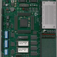
MPC555CME Freescale Semiconductor, MPC555CME Datasheet - Page 84

MPC555CME
Manufacturer Part Number
MPC555CME
Description
KIT EVALUATION FOR MPC555
Manufacturer
Freescale Semiconductor
Type
Microcontrollerr
Datasheet
1.MPC555CME.pdf
(966 pages)
Specifications of MPC555CME
Contents
Module Board, Installation Guide, Power Supply, Cable, Software and more
Processor To Be Evaluated
MPC555
Data Bus Width
32 bit
Interface Type
RS-232
For Use With/related Products
MPC555
Lead Free Status / RoHS Status
Contains lead / RoHS non-compliant
- Current page: 84 of 966
- Download datasheet (13Mb)
2.3.5.7 AN[52:54]/MA[0:2]/PQA[0:2]_[A:B]
2.3.5.8 AN[55:59]/PQA[3:7]_[A:B]
2.3.5.9 VRH
2.3.5.10 VRL
2.3.5.11 VDDA
2.3.5.12 VSSA
2.3.6 TOUCAN_A/TOUCAN_B PADS
2.3.6.1 CNTX0_[A:B]
MPC555
USER’S MANUAL
Pin Name: a_an52_ma0_pqa0 – a_an54_ma2_pqa2 (3 pins for first QADC),
b_an52_ma0_pqa0 – b_an54_ma2_pqa2 (3 pins for second QADC).
Analog Input (AN[52:54]) – Input-only. The input is passed on as a separate signal
to the QADC.
Multiplexed Address (MA[0:2]) – Output. Provides a three-bit multiplexed address
output to the external multiplexer chip to allow selection of one of the eight inputs.
Port (PQA[0:2]) – Bi-directional.
Pin Name: a_an55_pqa3 - a_an59_pqa7 (5 pins for first QADC), b_an55_pqa3 –
b_an59_pqa7 (5 pins for second QADC).
Analog Input (AN[55:59]) – Input-only. The input is passed on as a separate signal
to the QADC.
Port (PQA[3:7]) – Bi-directional.
Pin Name: vrh
VRH – Input pin for high reference voltage for the QADC_A and QADC_B modules.
Pin Name: vrl
VRL – Input pin for low reference voltage for the QADC_A and QADC_B modules.
Pin Name: vdda
VDDA – Power supply input to analog subsystems of the QADC_A and QADC_B mod-
ules.
Pin Name: vssa
VSSA – Input. Ground level for analog subsystems of the QADC_A and QADC_B
modules.
Pin Name: a_cntx0 (1 pin for first CAN), b_cntx0 (1 pin for second CAN)
/
MPC556
SIGNAL DESCRIPTIONS
Rev. 15 October 2000
MOTOROLA
2-26
Related parts for MPC555CME
Image
Part Number
Description
Manufacturer
Datasheet
Request
R

Part Number:
Description:
MPC555 Interrupts
Manufacturer:
Freescale Semiconductor / Motorola
Datasheet:
Part Number:
Description:
Manufacturer:
Freescale Semiconductor, Inc
Datasheet:
Part Number:
Description:
Manufacturer:
Freescale Semiconductor, Inc
Datasheet:
Part Number:
Description:
Manufacturer:
Freescale Semiconductor, Inc
Datasheet:
Part Number:
Description:
Manufacturer:
Freescale Semiconductor, Inc
Datasheet:
Part Number:
Description:
Manufacturer:
Freescale Semiconductor, Inc
Datasheet:
Part Number:
Description:
Manufacturer:
Freescale Semiconductor, Inc
Datasheet:
Part Number:
Description:
Manufacturer:
Freescale Semiconductor, Inc
Datasheet:
Part Number:
Description:
Manufacturer:
Freescale Semiconductor, Inc
Datasheet:
Part Number:
Description:
Manufacturer:
Freescale Semiconductor, Inc
Datasheet:
Part Number:
Description:
Manufacturer:
Freescale Semiconductor, Inc
Datasheet:
Part Number:
Description:
Manufacturer:
Freescale Semiconductor, Inc
Datasheet:
Part Number:
Description:
Manufacturer:
Freescale Semiconductor, Inc
Datasheet:
Part Number:
Description:
Manufacturer:
Freescale Semiconductor, Inc
Datasheet:
Part Number:
Description:
Manufacturer:
Freescale Semiconductor, Inc
Datasheet:


