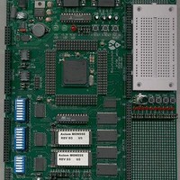
MPC555CME Freescale Semiconductor, MPC555CME Datasheet - Page 177

MPC555CME
Manufacturer Part Number
MPC555CME
Description
KIT EVALUATION FOR MPC555
Manufacturer
Freescale Semiconductor
Type
Microcontrollerr
Datasheet
1.MPC555CME.pdf
(966 pages)
Specifications of MPC555CME
Contents
Module Board, Installation Guide, Power Supply, Cable, Software and more
Processor To Be Evaluated
MPC555
Data Bus Width
32 bit
Interface Type
RS-232
For Use With/related Products
MPC555
Lead Free Status / RoHS Status
Contains lead / RoHS non-compliant
- Current page: 177 of 966
- Download datasheet (13Mb)
4.1 Burst Buffer Block Diagram
MPC555 / MPC556
USER’S MANUAL
The burst buffer module consists of the burst buffer controller (BBC) and the instruc-
tion memory protection unit (IMPU).
The BBC delivers the RCPU instruction fetch accesses from the instruction bus onto
the U-bus. It utilizes the full U-bus pipeline and a special page access attribute in order
to take full advantage of the U-bus bandwidth. It can handle both burstable and non-
burstable external memories as well as non-burstable internal memories (flash EE-
PROM, SRAM).
Code compression features are only available on the MPC556. The MPC556 utilizes
a version of code compression / decompression which is called “Phase A”. Phase A
code compression / decompression is described in this manual. Future parts may have
a different type of code compression. The BBC also contains the functional module
which is called the instruction code decompressor unit (ICDU). The ICDU is responsi-
ble for on-line (previously compressed) instruction code decompression in the “De-
compression-ON” mode. In the “Decompression-OFF” mode, the ICDU is bypassed
and the BBC is in normal function.
The IMPU allows the memory to be divided into four regions with different attributes,
as well as a default global region (for memory space that is not included in either of the
two regions). Each of the two regions can be of size four Kbytes to four Gbytes. Over-
lap between regions is allowed.
The IMPU includes registers that contain the following information: region base ad-
dress, region size and the region’s access permissions. For each access (from the
processor to the memory), the IMPU finds which region matches the address. If more
than one region matches, the region with the lowest index is chosen. If no region is
matched, the global region is chosen.
The IMPU compares the attributes of the access from the processor to the attributes
of the appropriate region. If the access is allowed, the proper signals are sent to the
BBC. If the access is not permitted, an interrupt is sent to the processor.
The IMPU does not support address translation. The effective fetch address issued by
the processor is the one that is transferred to the U-bus.
Figure 4-1
is a block diagram of the burst buffer.
BURST BUFFER
Rev. 15 October 2000
BURST BUFFER
SECTION 4
MOTOROLA
4-1
Related parts for MPC555CME
Image
Part Number
Description
Manufacturer
Datasheet
Request
R

Part Number:
Description:
MPC555 Interrupts
Manufacturer:
Freescale Semiconductor / Motorola
Datasheet:
Part Number:
Description:
Manufacturer:
Freescale Semiconductor, Inc
Datasheet:
Part Number:
Description:
Manufacturer:
Freescale Semiconductor, Inc
Datasheet:
Part Number:
Description:
Manufacturer:
Freescale Semiconductor, Inc
Datasheet:
Part Number:
Description:
Manufacturer:
Freescale Semiconductor, Inc
Datasheet:
Part Number:
Description:
Manufacturer:
Freescale Semiconductor, Inc
Datasheet:
Part Number:
Description:
Manufacturer:
Freescale Semiconductor, Inc
Datasheet:
Part Number:
Description:
Manufacturer:
Freescale Semiconductor, Inc
Datasheet:
Part Number:
Description:
Manufacturer:
Freescale Semiconductor, Inc
Datasheet:
Part Number:
Description:
Manufacturer:
Freescale Semiconductor, Inc
Datasheet:
Part Number:
Description:
Manufacturer:
Freescale Semiconductor, Inc
Datasheet:
Part Number:
Description:
Manufacturer:
Freescale Semiconductor, Inc
Datasheet:
Part Number:
Description:
Manufacturer:
Freescale Semiconductor, Inc
Datasheet:
Part Number:
Description:
Manufacturer:
Freescale Semiconductor, Inc
Datasheet:
Part Number:
Description:
Manufacturer:
Freescale Semiconductor, Inc
Datasheet:


