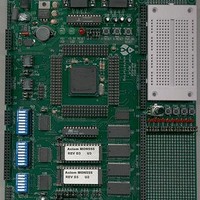
MPC555CME Freescale Semiconductor, MPC555CME Datasheet - Page 817

MPC555CME
Manufacturer Part Number
MPC555CME
Description
KIT EVALUATION FOR MPC555
Manufacturer
Freescale Semiconductor
Type
Microcontrollerr
Datasheet
1.MPC555CME.pdf
(966 pages)
Specifications of MPC555CME
Contents
Module Board, Installation Guide, Power Supply, Cable, Software and more
Processor To Be Evaluated
MPC555
Data Bus Width
32 bit
Interface Type
RS-232
For Use With/related Products
MPC555
Lead Free Status / RoHS Status
Contains lead / RoHS non-compliant
- Current page: 817 of 966
- Download datasheet (13Mb)
MPC555 / MPC556
USER’S MANUAL
The functions in the Bank 1 entry table are identical to the Bank 0 entry table functions
with three exceptions. Function 1, SPWM, has been replaced by RWTPIN. This is a
function that allows reads and writes to the TPU time bases and corresponding pin.
Function 5, PPWA, is now an identification function in
revision number is provided by this function. Finally, Function 7, MCPWM, has been
removed and left open for future use.
The CPU selects which entry table to use by setting the ETBANK field in the
TPUMCR2 register. This register is write once after reset. Although one entry table is
specified at start-up, it is possible, in some cases, to use functions from both
tables without resetting the microcontroller. A customer may, for example, wish to use
the ID function from Bank 1 to verify the TPU microcode version but then use the MCP-
WM function from Bank 0. As a customer will typically only run the ID function during
system configuration, and not again after that, the Bank 1 entry table can be changed
to the Bank 0 entry table using the soft reset feature of the TPU3. The procedure
should be:
The TPU3 stays in reset until the CPU clears the SOFTRST bit. After the SOFTRST
bit has been cleared the TPU3 will be reset and the entry table in Bank 0 will be se-
lected by default. To select the Bank 0 entry table, write 0b00 to the ETBANK field in
1. Set ETBANK field in TPUMCR2 to 0b01 to select the entry table in Bank 1
2. Run the ID function
3. Stop the TPU3 by setting the STOP bit in the TPUMCR to one.
4. Reset the TPU3 by setting the SOFTRST bit in the TPUMCR2 register
5. Wait at least nine clocks
6. Clear the SOFTRST bit in the TPUMCR2 register
Function
Number
0xD
0xC
0xE
0xB
0xA
0xF
9
8
7
6
5
4
3
2
1
0
Nickname
Function
Reserved
RWTPIN
COMM
HALLD
UART
QOM
PWM
SIOP
NITC
TSM
FQM
FQD
PTA
DIO
Table D-2 Bank 1 Functions
OC
ID
TPU ROM FUNCTIONS
Rev. 15 October 2000
Programmable Time Accumulator
Queued Output Match
Table Stepper Motor
Frequency Measurement
Universal Asynchronous Receiver/Transmitter
New Input Capture/Input Transition Counter
Multiphase Motor Commutation
Hall Effect Decode
Fast Quadrature Decode
Identification
Output Compare
Pulse Width Modulation
Discrete Input/Output
Read/Write Timers and Pin
Serial Input/output Port
Function Name
Table
D-2. The microcode ROM
MOTOROLA
D-3
Related parts for MPC555CME
Image
Part Number
Description
Manufacturer
Datasheet
Request
R

Part Number:
Description:
MPC555 Interrupts
Manufacturer:
Freescale Semiconductor / Motorola
Datasheet:
Part Number:
Description:
Manufacturer:
Freescale Semiconductor, Inc
Datasheet:
Part Number:
Description:
Manufacturer:
Freescale Semiconductor, Inc
Datasheet:
Part Number:
Description:
Manufacturer:
Freescale Semiconductor, Inc
Datasheet:
Part Number:
Description:
Manufacturer:
Freescale Semiconductor, Inc
Datasheet:
Part Number:
Description:
Manufacturer:
Freescale Semiconductor, Inc
Datasheet:
Part Number:
Description:
Manufacturer:
Freescale Semiconductor, Inc
Datasheet:
Part Number:
Description:
Manufacturer:
Freescale Semiconductor, Inc
Datasheet:
Part Number:
Description:
Manufacturer:
Freescale Semiconductor, Inc
Datasheet:
Part Number:
Description:
Manufacturer:
Freescale Semiconductor, Inc
Datasheet:
Part Number:
Description:
Manufacturer:
Freescale Semiconductor, Inc
Datasheet:
Part Number:
Description:
Manufacturer:
Freescale Semiconductor, Inc
Datasheet:
Part Number:
Description:
Manufacturer:
Freescale Semiconductor, Inc
Datasheet:
Part Number:
Description:
Manufacturer:
Freescale Semiconductor, Inc
Datasheet:
Part Number:
Description:
Manufacturer:
Freescale Semiconductor, Inc
Datasheet:


