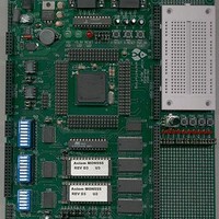
MPC555CME Freescale Semiconductor, MPC555CME Datasheet - Page 474

MPC555CME
Manufacturer Part Number
MPC555CME
Description
KIT EVALUATION FOR MPC555
Manufacturer
Freescale Semiconductor
Type
Microcontrollerr
Datasheet
1.MPC555CME.pdf
(966 pages)
Specifications of MPC555CME
Contents
Module Board, Installation Guide, Power Supply, Cable, Software and more
Processor To Be Evaluated
MPC555
Data Bus Width
32 bit
Interface Type
RS-232
For Use With/related Products
MPC555
Lead Free Status / RoHS Status
Contains lead / RoHS non-compliant
- Current page: 474 of 966
- Download datasheet (13Mb)
DDRQS — PORTQS Data Direction Register
14.6.3 PORTQS Data Direction Register (DDRQS)
MPC555
USER’S MANUAL
SET:
MSB
RE-
0
Bit(s)
8:15
DDRQS assigns QSPI pin as an input or an output regardless of whether the QSPI
submodule is enabled or disabled. All QSPI pins are configured during reset as gen-
eral-purpose inputs.
This register does not affect SCI operation. The TXD1 and TXD2 remain output pins
dedicated to the SCI submodules, and the RXD1, RXD2 and ECK pins remain input
pins dedicated to the SCI submodules.
*See bit descriptions in
0
1
2
3
4
5
6
7
1
/
MPC556
QPAPCS3
QPAPCS2
QPAPCS1
QPAPCS0
QPAMOSI
QPAMISO
DDRQS
2
Name
—
—
PQSPAR*
3
Table
Reserved
0 = Pin is assigned QGPIO3
1 = Pin is assigned PCS3 function
0 = Pin is assigned QGPIO2
1 = Pin is assigned PCS2 function
0 = Pin is assigned QGPIO1
1 = Pin is assigned PCS1 function
0 = Pin is assigned QGPIO0
1 = Pin is assigned PCS[0] function
Reserved
0 = Pin is assigned QGPIO5
1 = Pin is assigned MOSI function
0 = Pin is assigned QGPIO4
1 = Pin is assigned MISO function
PORSTQS data direction register. See
(DDRQS).
4
Table 14-10 PQSPAR Bit Descriptions
QUEUED SERIAL MULTI-CHANNEL MODULE
14-10.
5
Rev. 15 October 2000
6
7
8
0
0
PCS3
QDD-
Description
9
0
14.6.3 PORTQS Data Direction Register
QDD-
PCS2
10
0
QDD-
PCS1
11
0
PCS0
QDD-
12
0
QDD-
SCK
13
0
0x30 5016
QDD-
MOSI
MOTOROLA
14
0
14-12
QDD-
MISO
LSB
15
0
Related parts for MPC555CME
Image
Part Number
Description
Manufacturer
Datasheet
Request
R

Part Number:
Description:
MPC555 Interrupts
Manufacturer:
Freescale Semiconductor / Motorola
Datasheet:
Part Number:
Description:
Manufacturer:
Freescale Semiconductor, Inc
Datasheet:
Part Number:
Description:
Manufacturer:
Freescale Semiconductor, Inc
Datasheet:
Part Number:
Description:
Manufacturer:
Freescale Semiconductor, Inc
Datasheet:
Part Number:
Description:
Manufacturer:
Freescale Semiconductor, Inc
Datasheet:
Part Number:
Description:
Manufacturer:
Freescale Semiconductor, Inc
Datasheet:
Part Number:
Description:
Manufacturer:
Freescale Semiconductor, Inc
Datasheet:
Part Number:
Description:
Manufacturer:
Freescale Semiconductor, Inc
Datasheet:
Part Number:
Description:
Manufacturer:
Freescale Semiconductor, Inc
Datasheet:
Part Number:
Description:
Manufacturer:
Freescale Semiconductor, Inc
Datasheet:
Part Number:
Description:
Manufacturer:
Freescale Semiconductor, Inc
Datasheet:
Part Number:
Description:
Manufacturer:
Freescale Semiconductor, Inc
Datasheet:
Part Number:
Description:
Manufacturer:
Freescale Semiconductor, Inc
Datasheet:
Part Number:
Description:
Manufacturer:
Freescale Semiconductor, Inc
Datasheet:
Part Number:
Description:
Manufacturer:
Freescale Semiconductor, Inc
Datasheet:


