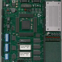
MPC555CME Freescale Semiconductor, MPC555CME Datasheet - Page 290

MPC555CME
Manufacturer Part Number
MPC555CME
Description
KIT EVALUATION FOR MPC555
Manufacturer
Freescale Semiconductor
Type
Microcontrollerr
Datasheet
1.MPC555CME.pdf
(966 pages)
Specifications of MPC555CME
Contents
Module Board, Installation Guide, Power Supply, Cable, Software and more
Processor To Be Evaluated
MPC555
Data Bus Width
32 bit
Interface Type
RS-232
For Use With/related Products
MPC555
Lead Free Status / RoHS Status
Contains lead / RoHS non-compliant
- Current page: 290 of 966
- Download datasheet (13Mb)
MPC555
USER’S MANUAL
Bit(s)
13:14
16:17
18:23
10
11
12
15
/
MPC556
ENGDIV
PRQEN
RTSEL
EECLK
Name
BUCS
EBDF
LME
Table 8-9 SCCR Bit Descriptions (Continued)
Power management request enable
0 = Remains in the lower frequency (defined by DFNL) even if the power management bit in
1 = Switches to high frequency (defined by DFNH) when the power management bit in the
RTC circuit input source select. At power-on reset RTSEL receives the value of the
MODCK1 bit. Note that if the chip is operating in limp mode (BUCS = 0), the RTSEL bit is
ignored, and the backup clock is the clock source for the RT and PIT clocks
0 = OSCM clock is selected as input to RTC and PIT
1 = EXTCLK clock is selected as the RTC and PIT clock source
Backup clock status. This status bit indicates the current system clock source. When loss of
clock is detected and the LME bit is set, the clock source is the backup clock and this bit is
set. When the user sets the STBUC bit and LME bit is set, the system switches to the backup
clock and BUCS is set.
0 = System clock is not the backup clock
1 = System clock is the backup clock
External bus division factor. These bits define the frequency division factor between (GCLK1
and GCLK2) and (GCLK1_50 and GCLK2_50). CLKOUT is similar to GCLK2_50. The
GCLK2_50 and GCKL1_50 are used by the external bus interface and memory controller in
order to interface to the external system. The EBDF bits are initialized during hard reset us-
ing the hard reset configuration mechanism.
00 = CLKOUT is GCKL2 divided by 1
01 = CLKOUT is GCKL2 divided by 2
1x = Reserved
Limp mode enable. When LME is set, the loss-of-clock monitor is enabled and any detection
of loss of clock will switch the system clock automatically to backup clock. It is also possible
to switch to the backup clock by setting the STBUC bit.
If LME is cleared, the option of using limp mode is disabled. The loss of clock detector is not
active, and any write to STBUC is ignored.
The LME bit is writable once, by software, after power-on reset, when the system clock is not
backup clock (BUCS = 0). During power-on reset, the value of LME is determined by the
MODCK[1:3] bits. (Refer to
0 = Limp mode disabled
1 = Limp mode enabled
Enable engineering clock. This field controls the output buffer strength of the ENGCLK pin.
When both bits are set the ENGCLK pin is held in the high state. These bits can be dynam-
ically changed without generating spikes on the ENGCLK pin. If ENGCLK is not connected
to external circuits, set both bits (disabling ENGCLK) to minimize noise and power dissipa-
tion. For measurement purposes the backup clock (BUCLK) can be driven externally on the
ENGCLK pin.
00 = Engineering clock enabled, full-strength output buffer
01 = Engineering clock enabled, half-strength output buffer
10 = BUCLK is the output on the ENGCLK full-strength output buffer
11 = Engineering clock disabled
Engineering clock division factor. These bits define the frequency division factor between
VCO/2 and ENGCLK. The divider ratio is ENGDIV+1. Division factor can be from 1 (ENGDIV
= 0b000000) to 64 (ENGDIV = 0b111111). These bits can be read and written at any time.
They are not affected by hard reset but are cleared during power-on reset.
NOTE: If the engineering clock division factor is not a power of two, synchronization between
the system and ENGCLK is not guaranteed.
NOTE: The default (Power On Reset) value of ENGDIV will be 0b111111 on all mask sets
after K62N. The default for previous mask sets (J76N, K02A, and K83H) is 0b000001.
the MSR is reset (normal operational mode) or if there is a pending interrupt from the
interrupt controller
MSR is reset (normal operational mode) or there is a pending interrupt from the interrupt
controller
CLOCKS AND POWER CONTROL
Rev. 15 October 2000
Table
8-1.)
Description
MOTOROLA
8-30
Related parts for MPC555CME
Image
Part Number
Description
Manufacturer
Datasheet
Request
R

Part Number:
Description:
MPC555 Interrupts
Manufacturer:
Freescale Semiconductor / Motorola
Datasheet:
Part Number:
Description:
Manufacturer:
Freescale Semiconductor, Inc
Datasheet:
Part Number:
Description:
Manufacturer:
Freescale Semiconductor, Inc
Datasheet:
Part Number:
Description:
Manufacturer:
Freescale Semiconductor, Inc
Datasheet:
Part Number:
Description:
Manufacturer:
Freescale Semiconductor, Inc
Datasheet:
Part Number:
Description:
Manufacturer:
Freescale Semiconductor, Inc
Datasheet:
Part Number:
Description:
Manufacturer:
Freescale Semiconductor, Inc
Datasheet:
Part Number:
Description:
Manufacturer:
Freescale Semiconductor, Inc
Datasheet:
Part Number:
Description:
Manufacturer:
Freescale Semiconductor, Inc
Datasheet:
Part Number:
Description:
Manufacturer:
Freescale Semiconductor, Inc
Datasheet:
Part Number:
Description:
Manufacturer:
Freescale Semiconductor, Inc
Datasheet:
Part Number:
Description:
Manufacturer:
Freescale Semiconductor, Inc
Datasheet:
Part Number:
Description:
Manufacturer:
Freescale Semiconductor, Inc
Datasheet:
Part Number:
Description:
Manufacturer:
Freescale Semiconductor, Inc
Datasheet:
Part Number:
Description:
Manufacturer:
Freescale Semiconductor, Inc
Datasheet:


