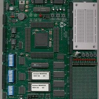
MPC555CME Freescale Semiconductor, MPC555CME Datasheet - Page 74

MPC555CME
Manufacturer Part Number
MPC555CME
Description
KIT EVALUATION FOR MPC555
Manufacturer
Freescale Semiconductor
Type
Microcontrollerr
Datasheet
1.MPC555CME.pdf
(966 pages)
Specifications of MPC555CME
Contents
Module Board, Installation Guide, Power Supply, Cable, Software and more
Processor To Be Evaluated
MPC555
Data Bus Width
32 bit
Interface Type
RS-232
For Use With/related Products
MPC555
Lead Free Status / RoHS Status
Contains lead / RoHS non-compliant
- Current page: 74 of 966
- Download datasheet (13Mb)
2.3.1.17 RSTCONF/TEXP
2.3.1.18 OE
2.3.1.19 BI/STS
2.3.1.20 CS[0:3]
MPC555
USER’S MANUAL
Transfer Error Acknowledge – This signal indicates that a bus error occurred in the
current transaction. The MCU asserts this signal when the bus monitor does not detect
a bus cycle termination within a reasonable amount of time. The assertion of TEA
causes the termination of the current bus cycle, regardless of the state of TEA. An ex-
ternal pull-up device is required to negate TEA quickly, before a second error is de-
tected. That is, the pin must be pulled up within one clock cycle of the time it was three-
stated by the MPC555 / MPC556.
Pin Name: rstconf_b_texp
Reset Configuration – Input. This input line is sampled by the chip during the asser-
tion of the HRESET signal in order to sample the reset configuration. If the line is as-
serted, the configuration mode will be sampled from the external data bus. When this
line is negated, the configuration mode adopted by the chip will be the default one.
Timer Expired – This output line reflects the status of the TEXPS bit in the PLPRCR
register in the USIU. This indicates an expired timer value.
Pin Name: oe_b
Output Enable – This output line is asserted when a read access to an external slave
controlled by the GPCM in the memory controller is initiated by the chip.
Pin Name: bi_b_sts_b
Burst Inhibit – This bi-directional, active low, three-state line indicates that the slave
device addressed in the current burst transaction is not able to support burst transfers.
When the chip drives out the signal for a specific transaction, it asserts or negates BI
during the transaction according to the value specified by the user in the appropriate
control registers. Negation of the signal occurs after the end of the transaction followed
by the immediate three-state. This pin is an active negate signal and may need an ex-
ternal pull-up resistor to ensure proper operation and signal timing specifications.
Special Transfer Start – This output signal is driven by the chip to indicate the start
of a transaction on the external bus or signals the beginning of an internal transaction
in showcycle mode.
Pin Name: cs0_b - cs3_b (4 pins)
Chip Select – These output signals enable peripheral or memory devices at pro-
grammed addresses if defined appropriately in the memory controller. CS0 can be
configured to be the global chip select for the boot device.
/
MPC556
SIGNAL DESCRIPTIONS
Rev. 15 October 2000
MOTOROLA
2-16
Related parts for MPC555CME
Image
Part Number
Description
Manufacturer
Datasheet
Request
R

Part Number:
Description:
MPC555 Interrupts
Manufacturer:
Freescale Semiconductor / Motorola
Datasheet:
Part Number:
Description:
Manufacturer:
Freescale Semiconductor, Inc
Datasheet:
Part Number:
Description:
Manufacturer:
Freescale Semiconductor, Inc
Datasheet:
Part Number:
Description:
Manufacturer:
Freescale Semiconductor, Inc
Datasheet:
Part Number:
Description:
Manufacturer:
Freescale Semiconductor, Inc
Datasheet:
Part Number:
Description:
Manufacturer:
Freescale Semiconductor, Inc
Datasheet:
Part Number:
Description:
Manufacturer:
Freescale Semiconductor, Inc
Datasheet:
Part Number:
Description:
Manufacturer:
Freescale Semiconductor, Inc
Datasheet:
Part Number:
Description:
Manufacturer:
Freescale Semiconductor, Inc
Datasheet:
Part Number:
Description:
Manufacturer:
Freescale Semiconductor, Inc
Datasheet:
Part Number:
Description:
Manufacturer:
Freescale Semiconductor, Inc
Datasheet:
Part Number:
Description:
Manufacturer:
Freescale Semiconductor, Inc
Datasheet:
Part Number:
Description:
Manufacturer:
Freescale Semiconductor, Inc
Datasheet:
Part Number:
Description:
Manufacturer:
Freescale Semiconductor, Inc
Datasheet:
Part Number:
Description:
Manufacturer:
Freescale Semiconductor, Inc
Datasheet:


