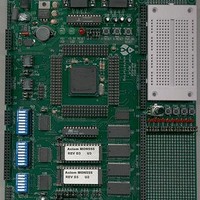
MPC555CME Freescale Semiconductor, MPC555CME Datasheet - Page 653

MPC555CME
Manufacturer Part Number
MPC555CME
Description
KIT EVALUATION FOR MPC555
Manufacturer
Freescale Semiconductor
Type
Microcontrollerr
Datasheet
1.MPC555CME.pdf
(966 pages)
Specifications of MPC555CME
Contents
Module Board, Installation Guide, Power Supply, Cable, Software and more
Processor To Be Evaluated
MPC555
Data Bus Width
32 bit
Interface Type
RS-232
For Use With/related Products
MPC555
Lead Free Status / RoHS Status
Contains lead / RoHS non-compliant
- Current page: 653 of 966
- Download datasheet (13Mb)
19.1 Introduction
MPC555 / MPC556
USER’S MANUAL
The two CDR MoneT flash EEPROM modules (CMF) serve as electrically program-
mable and erasable non-volatile memory (NVM) to store system program and data.
The modules are designed to be used with the unified bus (U-bus). The CMF arrays
use Motorola’s one-transistor (MoneT) bit cell technology. The MPC555 / MPC556’s
total 448-Kbytes of flash EEPROM non-volatile memory are distributed between two
CMF EEPROM modules: a 256-Kbyte array and a 192-Kbyte array. The erase block
size is 32 Kbytes.
Each CMF EEPROM module is arranged into two major sections. The first section is
the flash EEPROM array used to store system program and data. The second section
is the bus interface unit (BIU) that controls access and operation of the array through
a standard U-bus interface and the external signals EPEE (external program or erase
enable) and VPP (supply program or erase power).
Each CMF EEPROM module array is divided into blocks to allow for independent
erase, access state, and protection from program and erase for each block. Informa-
tion is transferred to the CMF EEPROM through the U-bus a word (32 bits), half-word
(16 bits), or byte at a time.
The BIU accesses 32 bytes of information in the array at a time. These bytes are cop-
ied into a read-page buffer aligned to the low order addresses, ADDR[27:31]. Each
CMF module contains two non-overlapping page buffers. The first page buffer is as-
sociated with array blocks zero to three. The second page is associated with array
blocks four to seven (for CMF Module A), or blocks four to five (for CMF Module B).
Read access time for data in the page buffers (on-page read) is one system clock. The
read access time for a new page of data (off-page read) is two system clocks. To pre-
vent the BIU from accessing an unnecessary page from the array, the CMF EEPROM
monitors the U-bus address to determine whether the required information is in one of
the two current pages and whether the access is valid for the module.
Burst accesses are not supported by the CMF EEPROM. In normal operation, write
accesses to the CMF array are not recognized.
The CMF EEPROM module requires an external program or erase voltage (VPP) to
program or erase the array or any of its control register shadow bits. Special hardware
interlocks and the external signal EPEE protect the array from accidental enabling of
program and erase operation. The program and erase algorithms are implemented by
a series of writes to the CMF EEPROM registers and are under software control.
CDR MoneT FLASH EEPROM
CDR MoneT FLASH EEPROM
Rev. 15 October 2000
SECTION 19
MOTOROLA
19-1
Related parts for MPC555CME
Image
Part Number
Description
Manufacturer
Datasheet
Request
R

Part Number:
Description:
MPC555 Interrupts
Manufacturer:
Freescale Semiconductor / Motorola
Datasheet:
Part Number:
Description:
Manufacturer:
Freescale Semiconductor, Inc
Datasheet:
Part Number:
Description:
Manufacturer:
Freescale Semiconductor, Inc
Datasheet:
Part Number:
Description:
Manufacturer:
Freescale Semiconductor, Inc
Datasheet:
Part Number:
Description:
Manufacturer:
Freescale Semiconductor, Inc
Datasheet:
Part Number:
Description:
Manufacturer:
Freescale Semiconductor, Inc
Datasheet:
Part Number:
Description:
Manufacturer:
Freescale Semiconductor, Inc
Datasheet:
Part Number:
Description:
Manufacturer:
Freescale Semiconductor, Inc
Datasheet:
Part Number:
Description:
Manufacturer:
Freescale Semiconductor, Inc
Datasheet:
Part Number:
Description:
Manufacturer:
Freescale Semiconductor, Inc
Datasheet:
Part Number:
Description:
Manufacturer:
Freescale Semiconductor, Inc
Datasheet:
Part Number:
Description:
Manufacturer:
Freescale Semiconductor, Inc
Datasheet:
Part Number:
Description:
Manufacturer:
Freescale Semiconductor, Inc
Datasheet:
Part Number:
Description:
Manufacturer:
Freescale Semiconductor, Inc
Datasheet:
Part Number:
Description:
Manufacturer:
Freescale Semiconductor, Inc
Datasheet:


